This thread has been locked.

If you have a related question, please click the "Ask a related question" button in the top right corner. The newly created question will be automatically linked to this question.

TPS65150: TPS65150

Part Number: TPS65150

Hi,sir

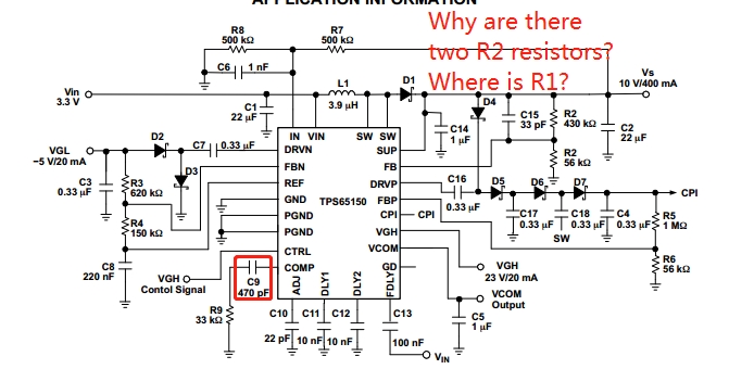
1.Vin=3.3V input. Why does Vin drop to 2.5 and produce large current when C9 is out of order or fails?

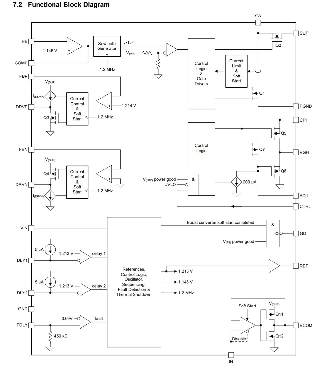
2.What's the gain of Amplifier? What is the ripple requirement for VFB?

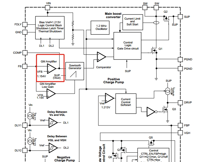
3.How does the regulating loop work?Does CFF correspond to C9?

  • Hello,

    Thank you for your post and I will be able to review in detail and provide any feedback by Monday, 12/14/2020.

    Kind Regards,

    Liaqat

  • Hello,

    Thank you for patience.

    1. C9 is the part of the compensation network for the internal feedback transconductance amplifier and when if it fails or is totally out of order value, it is possible to have an un-stable control loop possibly causing boost converter to oscillate. This could be what is causing the behavior that you are seeing.

    2.  Details of the internal circuits including amplifier gain are not available. Also, I believe you may be using an older datasheet. Please download the latest datasheet from the web and that may better clarify things.

    3. CFF correspond to C15 in the picture you showed. Again, I think you are using an older datasheet so I suggest to download latest which shows the application diagram copied below. This diagram also correctly shows R1 and R2 location. Figure 8 and the subsequent text describe operation of the control loop in the latest datasheet.

    Kind Regards,

    Liaqat