Other Parts Discussed in Thread: BQ76942, BQ76952
Hi TI Forum Team,
Currently i am working on TI BQ76942 EVM board . I communicate this (BQ76942 EVM) device with our Renesas RL78/F13(R5F10BGE) LQFP-48pin microcontroller over I2C protocol
Now i am able to communicate with this device to Our RL78/F13(R5F10BGE) microcontroller fine.
Also i abled to Read/Write the Following parameters :-
1. Cell Voltage Reading is completed.
2. Cell current Reading is completed.
3. Manufacturing Address Reading is completed.
4. Device ID Reading completed.
5. Read/Write Enable Protection A: Completed.
6. Able to ON/OFF the Charging/Discharging MOSFET completed.
My Problem:- These all above activity is completed fine with our source code. but when i try to Enable the "REG0 Config Enable" and "REG12 Config Enable" Register
with this same source code and the sequence of command is same as mentioned in the BQ76942 data sheet to Enable the both register and we do the same despite that i am not abled to Enable the REG1 & REG2 register to getting the voltage at this pin why?
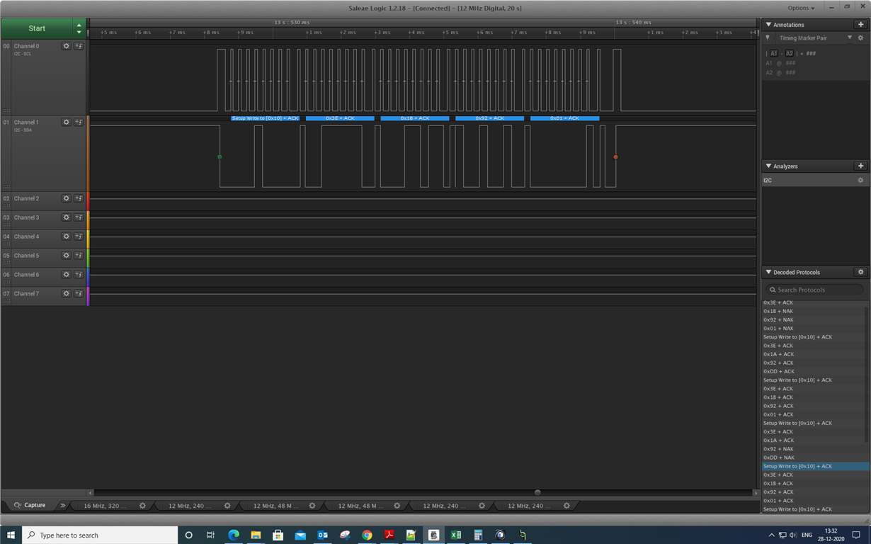
REG0 Config enable command and its sequence what i am sending over I2C protocol
//---REG0 Config Enable : Address=0x921B, Data =0x01(REG0_EN bit =1) [RSVD_0| RSVD_0| RSVD_0| RSVD_0| RSVD_0| RSVD_0| RSVD_0| REG0_EN]
TXbuff[0]=0x3E;
TXbuff[1]=0x1B;
TXbuff[2]=0x92;
TXbuff[3]=0x01; //(REG0_EN bit =1
//--Command sending Sequence Over I2C
StartCondition(); /* Start Condition */
ret=ByteWrite(0x10);
ret=ByteWrite(TXbuff[0]);
ret=ByteWrite(TXbuff[1]);
ret=ByteWrite(TXbuff[2]);
ret=ByteWrite(TXbuff[3]);
StopCondition();
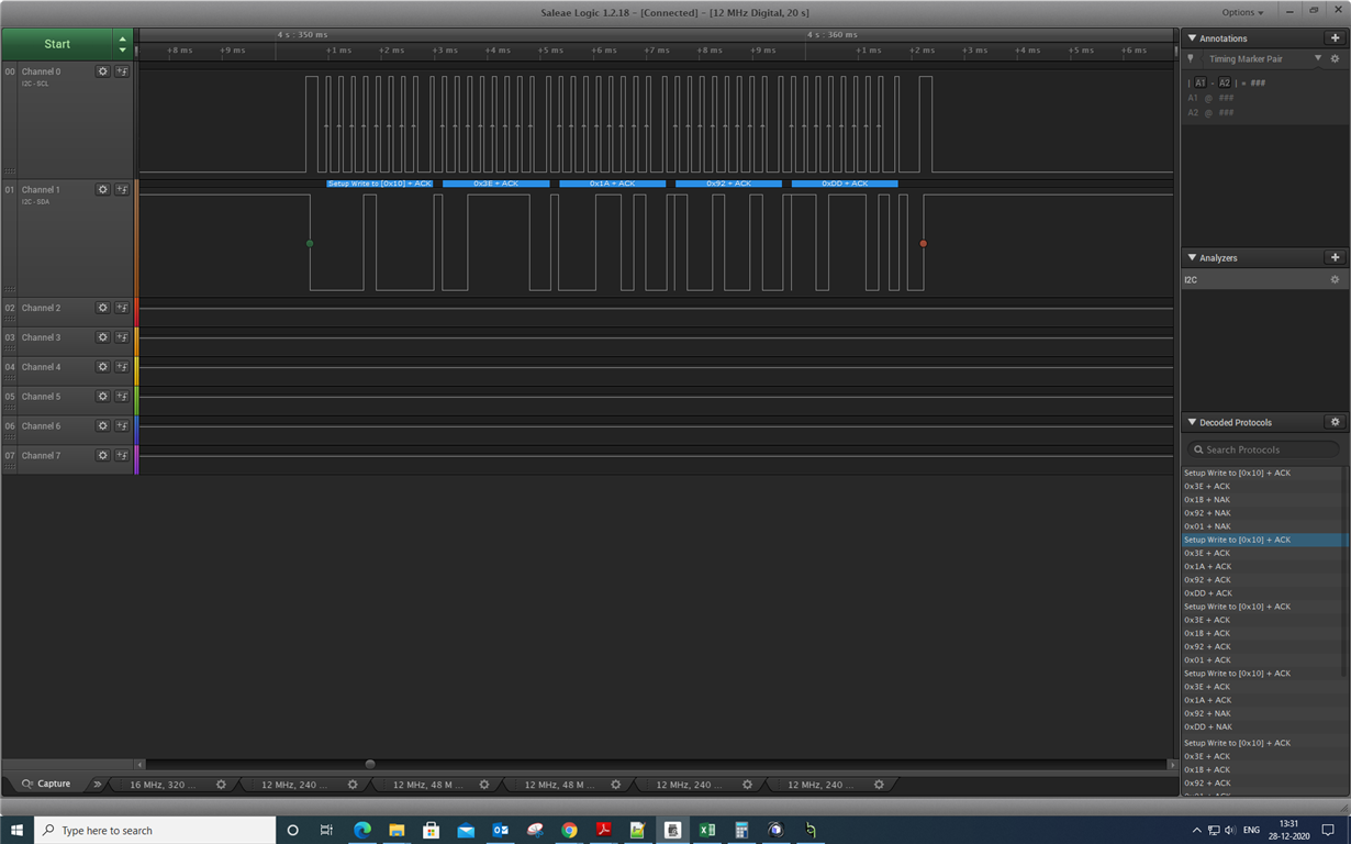
REG12 Config enable command and its sequence what i am sending over I2C protocol
//---REG12 Config Enable = 3.3V ,Address =0x921A ,Data=0xDD [REG2V_2| REG2V_1| REG2V_0| REG2_EN| REG1V_2| REG1V_1| REG1V_0| REG1_EN]
TXbuff[4]=0x3E;
TXbuff[5]=0x1A;
TXbuff[6]=0x92;
TXbuff[7]=0xDD;
StartCondition();
ret=ByteWrite(0x10);
ret=ByteWrite(TXbuff[4]);
ret=ByteWrite(TXbuff[5]);
ret=ByteWrite(TXbuff[6]);
ret=ByteWrite(TXbuff[7]);
StopCondition();
Result:- when i sending the above command & its sequence but REG1 and REG2 are not enabled(i.e. we not get voltage at this pin).
Note :- 1. Our source code is working fine for other parameters Reading/Writing.
2. I have doubt about the command & its sequence , so let me know where i am wrong ?
or what i should do to make/Invoke voltage at REG1 & REG2 pin on EVL board?
Please Refer the data captured through Logic Analyser:- 1. REG0 Config Enable Data Captured
2. REG12 Config Enable Data Captured
//-----------------------------------------------------------------------
//---REG0 Config Enable : Address=0x921B, Data =0x01(REG0_EN bit =1)[RSVD_0| RSVD_0| RSVD_0| RSVD_0| RSVD_0| RSVD_0| RSVD_0| REG0_EN]
TXbuff[0]=0x3E;
TXbuff[1]=0x1B;
TXbuff[2]=0x92;
TXbuff[3]=0x01;

//---REG12 Config Enable = 3.3V ,Address =0x921A ,Data=0xDD [REG2V_2| REG2V_1| REG2V_0| REG2_EN| REG1V_2| REG1V_1| REG1V_0| REG1_EN]
TXbuff[4]=0x3E;
TXbuff[5]=0x1A;
TXbuff[6]=0x92;
TXbuff[7]=0xDD;

while(1)
{
	        StartCondition();										/* Start Condition */
		ret=ByteWrite(0x10);
		ret=ByteWrite(TXbuff[0]);
		ret=ByteWrite(TXbuff[1]);
		ret=ByteWrite(TXbuff[2]);
		ret=ByteWrite(TXbuff[3]);
		StopCondition();
		Delay(80000);Delay(80000);

		StartCondition();
		ret=ByteWrite(0x10);
		ret=ByteWrite(TXbuff[4]);
		ret=ByteWrite(TXbuff[5]);
		ret=ByteWrite(TXbuff[6]);
		ret=ByteWrite(TXbuff[7]);
		StopCondition();
	       Delay(80000);Delay(80000);
}
////-------------------------------------------------------------------------------------


