This thread has been locked.

If you have a related question, please click the "Ask a related question" button in the top right corner. The newly created question will be automatically linked to this question.

TPS54060EVM-590: LM5017 in split rail configuration instead of fly-buck

Part Number: TPS54060EVM-590
Other Parts Discussed in Thread: LM5017

Hi,

I ultimately want to generate a +/-12VDC rail from +48VDC. The +/-12V split rail will power a couple of OP-amps and I also need 12V to power a separate cooling fan.

The TPS54060EVM-590 module did just that but I realized that in such a configuration, the TPS54060s max Vin is reached due to the fact that it sees 48V -(-12V) = 60V. This will be an issue since my 48VDC in might vary above +48V.

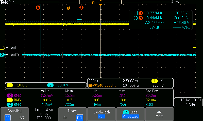
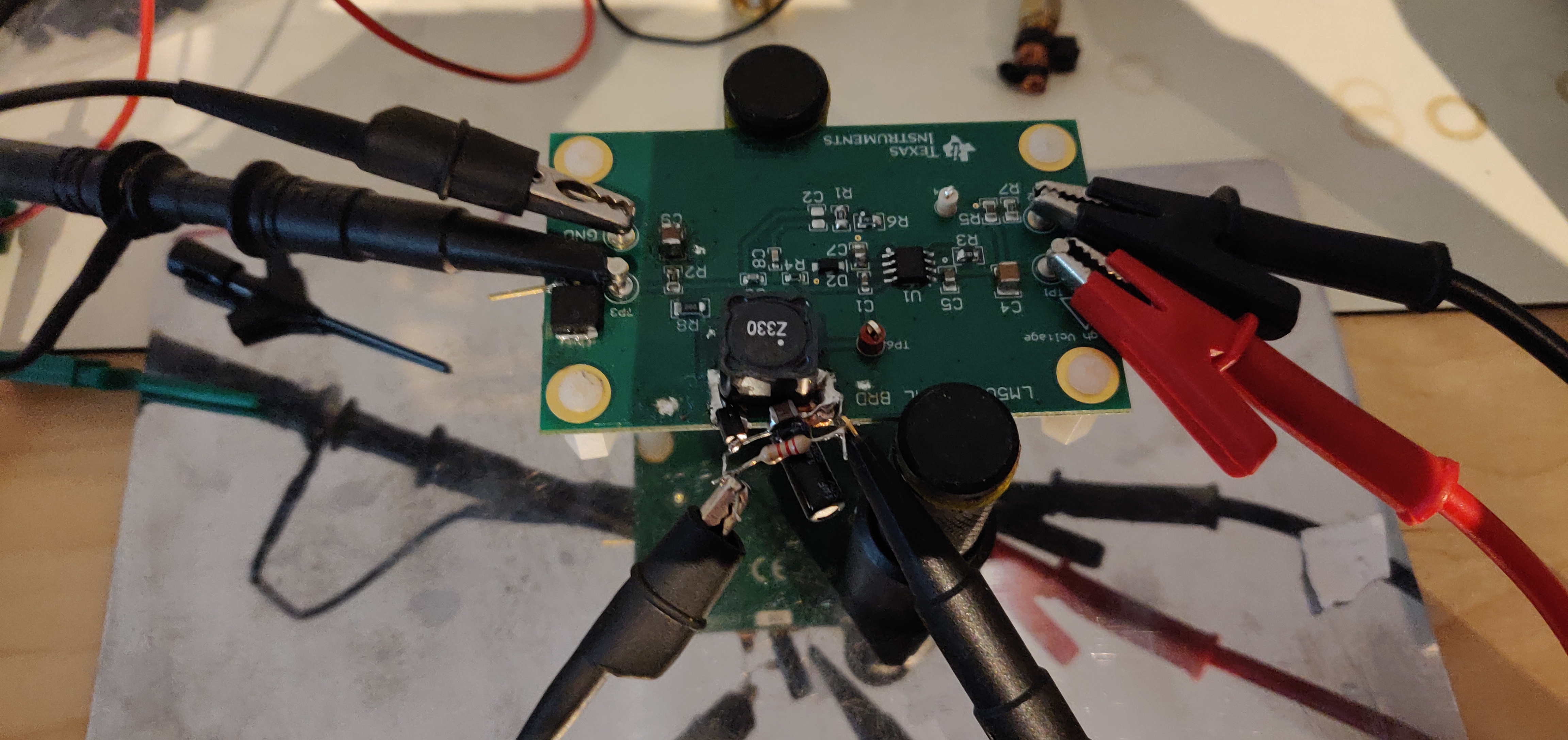
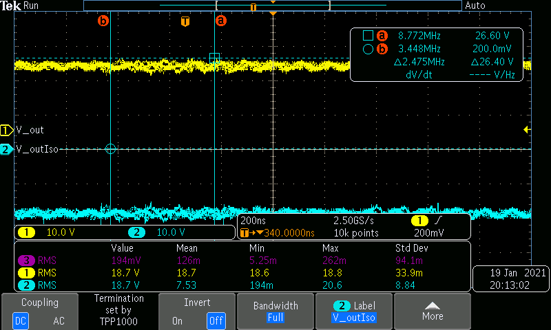
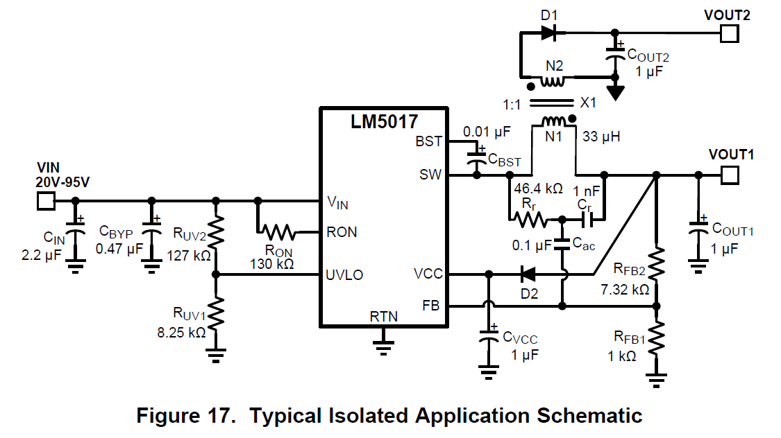
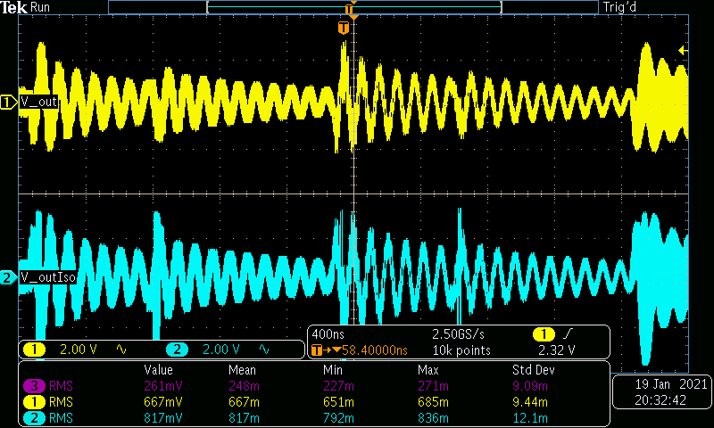
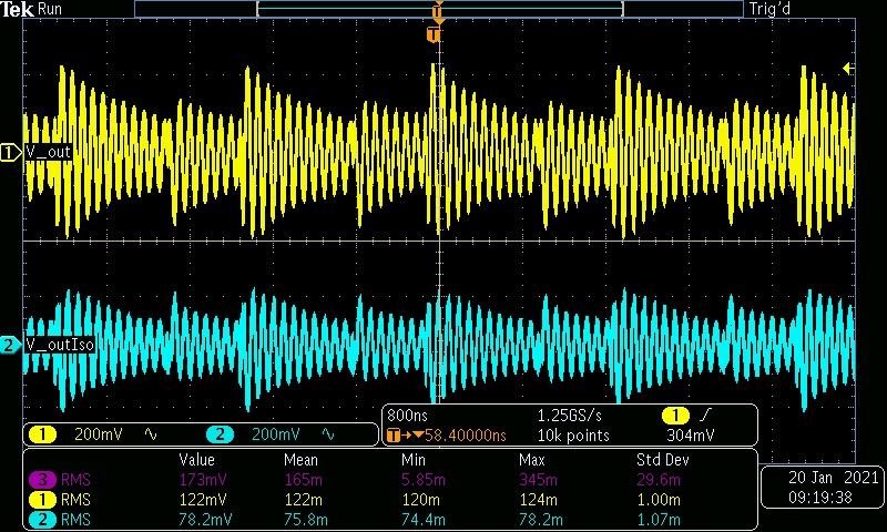
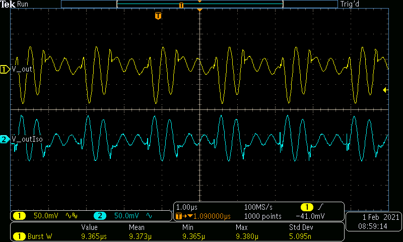
I have looked at the LM5017 in a fly-buck configuration since it can take up to 100V input voltage but I ran into problem when connecting the isolated output GND to the non-isolated GND.

Could you suggest a design that can create the desired +/-12V and withstand the high input voltage? Current output is up to 250mA on the +12V rail and up to 100mA on the -12V rail.

Best regards

  • Hello Erik,

    Can you elaborate on what the problem you ran into when using the LM5017?

    I would recommend to take a look at the following Application Note: Creating a Split-Rail Power Supply With a Wide Input Voltage Buck Regulator.
    The application note will demonstrate method on how to generate a positive and negative output power supply using a standard buck.

    Regards,
    Alejandro

  • Hi Alejandro,

    I introduced alot of unwanted voltage ripple on both the primary side and the secondary side when connecting the isolated "GND_iso" to GND.

    I have used the LM5017 EVAL board and replaced the original inductor with a coupled inductor to create the fly-buck topology:

    Below is a screenshot when only the primary, non isolated output  voltage rail is measured:

    When I connect the two voltage rails together by letting them share the same GND trough the oscilloscope as in the photo below:

    I get the following waveforms:

    If I remove the oscilloscope probe and GND clip from the primary voltage output, I get a much cleaner voltage at the isolated output:

    This is the schematic from the LM5017 datasheet that I have tried to follow as much as possible:

    The reason I have around +/-18V RMS output is that I intend to use some kind of LDO to provide a more stable +/-12VDC output.

    Please let me know if there is any obvius mistake that I have made.

  • Here is another screenshot with the oscilloscope ac-coupled to get a better view of the waveforms:

  • Hi Erik,

    Understood. I recommend to change to a better measuring technique. Improper measurement techniques can exaggerate the output noise. Take a look at the following:

    Regards,
    Alejandro

  • I do not think that just reducing the GND loops is the solution to my problems. Here is another measurement where I have removed the GND clips completely and I make the GND connection directly to the GND ring of the oscilloscope probe:

    And I still get pretty much the same measurement results:

  • The ripple is reduced alot but it is still very much there. My concern is why the ripple is introduced first when the isolated output and the primary output of the buck regulator are connected together with common GND

  • Erik,

    I understand. We just wanted to get a more realistic reading of the ripple.
    Let's try something: Place a "Y-CAP" as demonstrated in the following App Report. Something like a 2.2nF 2-kV cap from primary-GND to secondary-GND to redirect the current through the winding-winding capacitance.

    Thanks,
    Alejandro

  • ok, I will give that a try. Is there a reason for the 2kV rating?

    I only have 50V 2,2nF ceramic capacitors avalible at my desk currently.

    If needed I will order 2kV rated 

  • Hi Erik,

    It doesn't have to be 2-kV rated, but it has to be a Class-Y capacitor. And all y-caps (that I know of) are rated for high voltages.

    So, the emphasis would have to be please make sure it is a y-class cap.

    Regards,
    Alejandro

  • Hi Alejandro,

    I have now tried adding a 2.2nF, 2kV capacitor between the two voltage rails and I get the waveforms below when measuring both voltage rails at the same time:

    The capacitor reduces the voltage ripple further, but it is still clear that as soon as I connect the two voltage rails together with the oscilloscope gnd connections, the voltage ripple is worse than if I only measure one of the output rails at a time. (I am measuring with shortest possible gnd leads as before) 

    If I only measure one of the voltage outputs at a time, I get the waveforms below:

    This is  the datasheet for the capacitor I found (I am not 100% that it is actually a Y-class capacitor but this is what I could get hold of easily): 

    www.elfa.se/.../C1206C222KGRACTU_eng_tds.pdf

    I am currently supplying my test setup with 5pcs of 9V battery in series to get a clean input voltage and to eliminate the possibility that the supply voltage would introduce unwanted noice.

    Is there a way to further reduce the ripple when the two rails are connected together?

    Best regards

    Erik

  • Hi Erik,

    Good, as expected, the capacitors reduced the noise even further.

    I don't think this is a matter of converter noise anymore. Instead, I believe this is a matter of false display of apparent converter noise. You isolated your power supply, which means it is no longer line grounded. Have you tried isolating your scope?

    Regards,
    Alejandro

  • Hi Alejandro,

    Here is a screenshot from my oscilloscope after isolating the PE-connection in the mains connector:

    It does not seem to have any significant impact on reducing the measured voltage ripple.

    Altough the voltage ripple is sigificantly less with the added capacitor, 100mVpp seems a bit high still. 

    The measurement screenshots I have provided so far are taken with a 2k load on the isolated rail but with no load on the primary voltage output. I see almost no difference when drawing 0mA or 250mA current on the primary output.

  • Hi Erik,

    I would also like to point out the additional soldered components on your board (from previous images provided) might also be picking up a lot of noise. The long leads from the resistor seen and cap are picking up unwanted noise.
    As stated previously, I believe this is a false display of apparent convert noise.

    Regards,
    Alejandro