This thread has been locked.

If you have a related question, please click the "Ask a related question" button in the top right corner. The newly created question will be automatically linked to this question.

LM5109A: Charge pump operation at high temperature?

Part Number: LM5109A

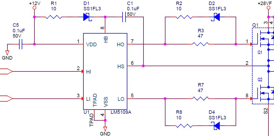
Hi, we have a small inverter for a BLDC motor that uses the LM5109A.  Commutation is six-step, and at temperatures above about 75C, the voltage on the charge pump capacitor is dropping about 3X faster than at room temperature.  It is dropping sufficiently fast to turn the high-side FET off prematurely.   All components are rated to 125C or better, and the charge pump capacitor is about 5X bigger than it should need to be at the frequency of operation (according to the equations in the LM5109A data sheet).  The capacitance should not change more than 15% maximum.

Does the internal charge pump circuitry on the LM5109A have increased leakage at high temperatures, or is there some other temperature dependency that may be causing this issue?

Thanks,

Neil

  • Hello Neil,

    Thanks for reaching out.

    If I understand the issue correctly, the HB_HS capacitor voltage is not maintaining sufficient voltage to keep the high-side FET voltage above the UVLO? This issue only occurs at T>75C? Please confirm. If that is correct, can you also confirm that HB-HS is replenishing sufficiently during the low-side turn-on time? Can you confirm that CVDD is sized such that CVDD >=10*C_hb_hs? 

    If available, kindly share your schematic.

    Regards,

    -Mamadou 

  • Hi Mamadou,

    Your understanding is correct, the HB-HS capacitor voltage is dropping faster than expected, and faster than it drops at room temperature.  Above 75C, it is insufficient to keep the high-side charge pump voltage above UVLO.  There is no performance issue at ~20C.  

    The CVDD bypass capacitors are a 0.1uF and a 4.7uF capacitor, which is greater than 10X the 0.1uF HB-HS capacitor.  The HB-HS capacitor voltage recharges as expected during the low-side turn on.  I'm attaching the relevant portion of the schematic, although it does not show the 4.7uF capacitor.

  • Hello Neil,

    Thanks for the schematic!

    I have few comments/questions.

    The total gate drive power is 2 x Qg x VDD x Fsw. With high external gate resistors sharing the power dissipated with the driver, the driver should not be reaching  the junction temperature should be close to the max operating range, please confirm.

    Also your boot diode appears to be a 30V diode while bus voltage is shown to be 28V, can you update this diode with wider margin such as 75V to 100V?

    It sounds like the boot cap is not replenishing fully causing the HB_HS cap to drain and dropping the gate voltage, can you please confirm the HB_HS during the "failure condition"? 

    We may also need to review the boot cap value based on the MOSFETs equivalent gate charge referring to Section 8.2.2.1 of the datasheet. Depending on the FETs load, have you tried increasing Cboot to 470nF and the CVDD caps accordingly? 

    Please try these suggestions and let us know if there are still issues.

    Regards,

    -Mamadou

  • Thanks for that Mamadou, it turns out that the reverse leakage of the diode increases by a factor of about 100X from room temperature to 100C.  That is about the right amount of additional leakage current to cause the effect we are seeing.  We will look for a different diode (most likely higher voltage rating) that has lower reverse leakage at that temperature.

    Neil