This thread has been locked.

If you have a related question, please click the "Ask a related question" button in the top right corner. The newly created question will be automatically linked to this question.

ISO5852S-EP: DESATs during shoot-through waveforms

Part Number: ISO5852S-EP
Other Parts Discussed in Thread: ISO5852S

[reposted due to photo display issue]

Hi TI representatives,

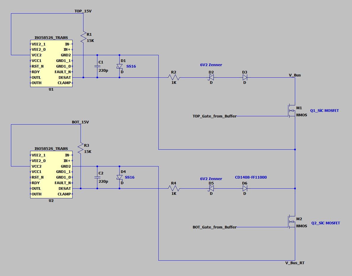
We are using ISO5852s for half-bridge SiC MOSFET. VDC bus is ~200V and target to trigger DSAT at Vds ~ 1.4V in less than 2 us.  The circuit snippet is as below:

The protection is working very well during shoot-through test when Q2 is pre-biased ON and then purposefully turn on Q1. Measurement of DSAT signals on both top/bottom Iso5852 shows interesting waveforms:

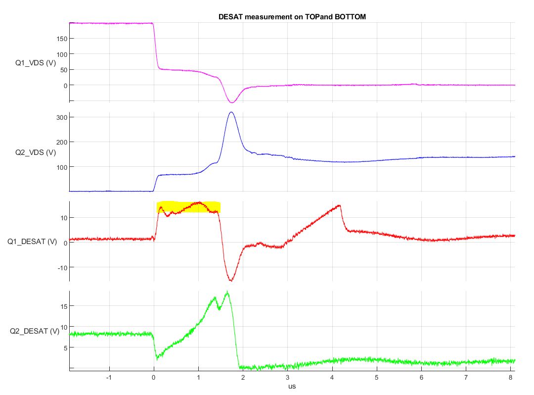
It seems like the Q2 triggers DESAT first, and that does make sense. But, I don't know why the Top DESAT misses the first trigger? The highlighted area is well above +9V in more than 1 us.

Any comment/thought is appreciated.

Thank you.

  • Hi Duc,

    Thank you for reaching out to E2E!

    I will look into this and provide an update by the EOD.

    Best regards,

    Andy Robles

  • Hi Duc,

    Looking at the waveforms they don't exactly make sense to me. Would be able to annotate on the schematic where exactly the signals plotted above are being probed with the reference point included? (i.e. right at the pins of the gate driver DESAT pins with reference to GND2, or a different location in the schematic?)

    Best regards,

    Andy Robles

  • Hi Andy,

    Thank you for the reply. Q1_DESAT/Q2_DESAT are measured across D1/D4 on the schematic respectively.

    Bests,

    Andy Robles said:

    Hi Duc,

    Looking at the waveforms they don't exactly make sense to me. Would be able to annotate on the schematic where exactly the signals plotted above are being probed with the reference point included? (i.e. right at the pins of the gate driver DESAT pins with reference to GND2, or a different location in the schematic?)

    Best regards,

    Andy Robles

  • Hi Duc,

    Our expert is reviewing the latest information and will get back to you promptly.

    Thanks for your patience.

    -Mamadou 

  • Hi Duc,

    I apologize for the delay. After running some simulations I noticed some abnormal behavior of the model when not all the pins were not properly connected. I see from the snippet you shared you simplified the schematic as to only show the signals in question. Would you be able to share the full schematic that gave the wave forms in question?

    One pin that is often ignored is the CLAMP pin. Even if the clamp function is not used be sure to connect it to VEE in the simulation to obtain proper results.

    Let me know if there's any questions.

    Best regards,

    Andy Robles

  • Hi Andy,

    The CLAMP pin is connected to the Gate of Mosfet that is not showing on the snippet. And the waveform is measured directly from hardware then extracted by MATLAB for better data analysis. Sorry for not be able to share the whole circuit for the sake of the project's confidential, but It is a typical gate drive topology with BJT totem-pole buffer. Everything else is working fine, I am not sure the problem can be duplicated on the simulation or not since the DESAT mechanism itself is pretty straightforward.

    And, not sure have you been reported anything which is similar to this before?

    Thank you,

    Duc.

  • Hi Duc,

    Looking at the actual schematic and waveforms could be useful as I have not seen something similar before.

    I have sent you a request to connect through E2E through which I shared my email in order to be able to share more confidential information that you do not wish to share here. I will go ahead and close this thread as we will continue our conversation over email.

    Best regards,

    Andy Robles

  • Thanks Andy,

    Yeah, you can close this thread and move on into email conversation.

    Duc.