This thread has been locked.

If you have a related question, please click the "Ask a related question" button in the top right corner. The newly created question will be automatically linked to this question.

TPS61097A-33: Boost does not work Issue & Schematic review

Part Number: TPS61097A-33

Hi

The customer was using the TPS61097A-33 for remote control.

TPS61097A Schematic : There is no problem with the boost action.

Input Voltage(VBAT) : 3V(AA*2)

Output Voltage : 3.3V

LED 1ea : 2mA 

We designed to add Voltage detector IC to turn on and off due to specification changes.

Additional Voltage detector Schematic : Boost does not work

- Input voltage(VBAT) 1.7V or less Cut-off

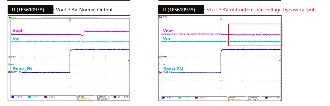
However, the Vout voltage of the TPS61097A is not 3.3V (BOOST up is not possible) and the Vin voltage is output to Vout as it is.

Competitor IM8132S has no problem with BOOST UP operation.

Please check the schematic for problems..

Schematic Attachment : 

PCB Layout : 

  • Hi,

    Updates additional reviews.

    I am sending you the output waveform comparison data from PCB(A) and PCB(B) of IMS and TI.

    The output waveform from PCB(B) shows that:

    After Boost_EN, the Vout voltage appears as if the Vin voltage is bypassed and the waveform is switched.

    Review Report : 

    The TPS61097A is used only for power back-lighting.

    The product specification covers the light sensor and presses the key to turn the back-light LED on and off for 5 seconds. (Last second slowly turns off with Dimming)

    In the last one-second interval, the back-light slowly turns off due to dimming and the current load gradually decreases, and V-out slowly rises from the bypass voltage.

    We can't find the cause of the problem.

  • Hi CHo:

    Please share the waveform of the TPS61097, Including the Vin, L, Vout and current of the inductance. Thank you! 

  • Hi Minqiu,

    I have attached a waveform.

    I'm sorry, but please review it as soon as possible.

    CH1 : VIN

    CH2 : VOUT

    CH3 : VL

    CH4 : IL

    PCB(A)_Normal operation 1 & PCB(A)_Normal operation 1-1 : Revision A PCB

    PCB(B)_PCB(A)_Bad operation 1 & PCB(B)_PCB(A)_Bad operation 1-1 : Revision B PCB

    TPS61097A Waveform.zip

  • Hi Cho:

    I afraid the converter maybe enter into the bypass mode. Please also check the EN pin status. And is there any other risk to lead this? 

    "The TPS61097 contains a P-channel MOSFET (Bypass Switch) in parallel with the synchronous rectifying MOSFET. When the IC is enabled (EN = VIH), the Bypass Switch is turned off to allow the IC to work as a standard boost converter. When the IC is disabled (EN = VIL) the Bypass Switch is turned on to provide a direct, low impedance connection from the input voltage (at the L pin) to the load (VOUT). The Bypass Switch is not impacted by Undervoltage lockout, Overvoltage or Thermal shutdown."

  • Hi Minqiu,

    The attached report has a waveform with a normal EN signal.

    Review Report :

  • Hi Cho:

    I checked the layout, it's bad. I afraid customer need to redo the PCB layout. Please follow the guidacne in the datasheet. 

    And for customer debug, I think the IC maybe damaged. They can replace one and put the Cout as close as possible to the IC.

  • Hi Minqiu,

    I'm sorry. I'm late to share information.

    We found the cause last Friday. Because it is a product that is being mass-produced, there are many problems such as 4M change, so sharing was delayed.

    The position of the output capacitor was moved close to the IC.

    The output was 3.3v and normal.

    The customer thinks that the TPS61097 product is too sensitive to the location of GND and CAPACITOR.

    Q1 : Please explain why the output capacitor should be located close to the IC.

  • Hi Cho:

    According to the layout, it's really far away and high risk. 

    For the reason, I will share some documents with you. Please check the page 8. www.ti.com/.../snva731.pdf

     And here is another guidance. https://www.ti.com/lit/slva773