This thread has been locked.

If you have a related question, please click the "Ask a related question" button in the top right corner. The newly created question will be automatically linked to this question.

TPS24720: Output does not rise with resistive load

Part Number: TPS24720
Other Parts Discussed in Thread: CSD17578Q3A

Schematic diagram of the relevant part:

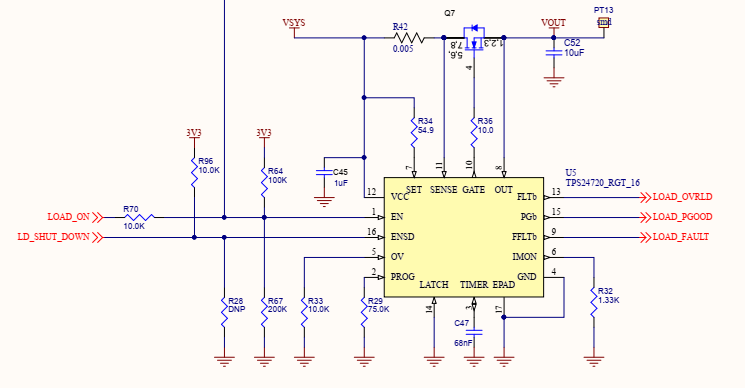
VSYS is 12V nominal.

When I connect a resistive load (4 Ohms), the overload protection is kicking in:

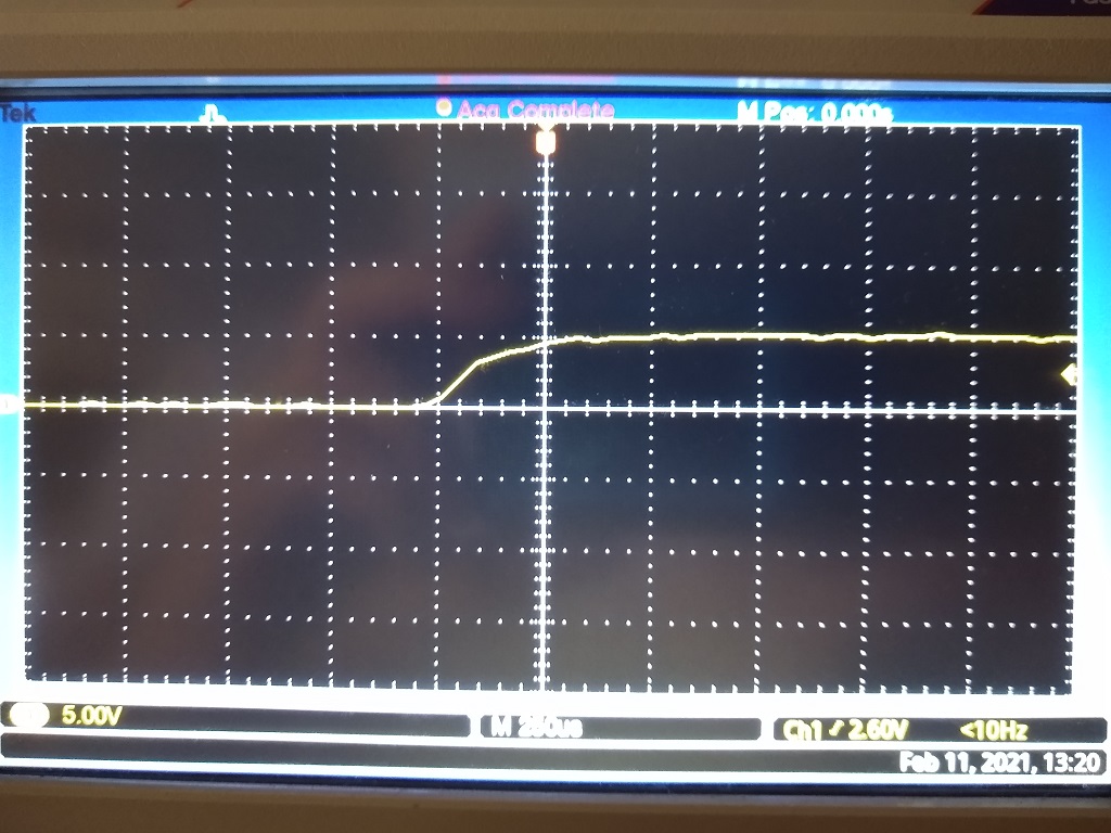
The switch retries after a few hundreds of ms and the pattern repeats. If I disconnect the resistance and enable the switch and connect the resistance back after VOUT settles, it works.

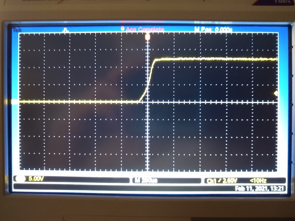
Per my calculations, the current limit is 5A and the fault timer is 10ms. 

With an electronic load set to the same resistance, I get

What am I missing?

  • Hi Elder,

    Thanks for reaching out to us. Please could you fill the design calculator and share with us. The design calculator is available at . Kindly help us to understand better by mentioning the signal name on the corresponding captured waveforms.

  • Hello, Avishek.
    First off, thank you very much for your prompt response to my inquiry in the forum and your support.
    About the signal in the capture waveforms, VOUT in all three cases. The second screenshot is from the same capture as the first one, only with the time scale of the oscilloscope zoomed in to detail the rising part of the waveform.
    While working on this post, I noticed on the waveform with the fixed resistor that VOUT stays fixed on 5V for 11ms and then it is zeroed. For some reason it cannot rise through 12V and so the fault timer kicks in and disables the FET. What I cannot understand is why, with the electronic load configured as a fixed 4R resistor, that does not happen (third screenshot). Any idea of the cause?
    Please find the spreadsheet partially filled with my design's parameter and I have set some inputs for the test setup I used to get the waveforms above. For example, the Maximum Output Load Capacitance is 10uF (the real load will have a few hundreds of uF).
    I followed the tutorials fill the spreadsheet in, but I got stuck on the fourth step (the fifth is not relevant to my application). I have some questions/comments listed below.
    1- What is Target Power Limit for? The tutorial shows the Minimum Power Limit calculated is copied on the line right below it. RPROG is calculated. In the spreadsheet, I used the actual value of RPROG in my design, wich makes actual PLIM higher.
     
    2- What is that Load Turn-on Threshold for? The tutorial talks about it but still I did not figure it out, and how it applies to my design. I am using the eswitch (for simplicity I will call the whole circuit eswitch) as a simple switch only, i.e., to power a load on/off (no hot swap). So, in my case, the input voltage is already stable at 12V when the eswitch is turned on. Should I still use 0V at that Load Turn-On threshold cell?
    3- I couldn't change the Load Turn-On Threshold cell, I get an error about the value, whatever I try, not meeting range restrictions.
    I hope you can help me with these questions.
    Once again, thank you very much for your support.
  • Hi Elder,

    Thanks a lot for providing all the information. We are working on this and will come back to you by tomorrow end of the day.

  • Hi Elder,

    Sorry for the delay in response. 

    1- What is Target Power Limit for? The tutorial shows the Minimum Power Limit calculated is copied on the line right below it. RPROG is calculated. In the spreadsheet, I used the actual value of RPROG in my design, which makes actual PLIM higher. Minimum power limit is defined by the accuracy of the internal circuitry due to the presence of offset voltages. Target power limit should always be more than the minimum one to have the accurate power limit during startup or fault. Higher power limit helps in startup with load. But, it reduces the margin on MOSFET SOA limit. Hence, the target power limit should be judiciously chosen taking care the aforementioned aspects.

    2- What is that Load Turn-on Threshold for? The tutorial talks about it but still I did not figure it out, and how it applies to my design. I am using the eswitch (for simplicity I will call the whole circuit eswitch) as a simple switch only, i.e., to power a load on/off (no hot swap). So, in my case, the input voltage is already stable at 12V when the eswitch is turned on. Should I still use 0V at that Load Turn-On threshold cell? As the Hot Swap controller is getting started with a resistive load, Load Turn-On threshold will be at 0V.

    3- I couldn't change the Load Turn-On Threshold cell, I get an error about the value, whatever I try, not meeting range restrictions. Please keep the turn on threshold at 0V.

    According to the mentioned application, power limit (PLIM) has to be more to successfully complete the startup inrush with a resistive load of 4Ω. Otherwise, it will trigger the fault timer. Hence, the power limit of 15W is considered and R29 needs to be changed to 47K from 75K.

    With this higher value of power limit, startup time (Tstart) will be reduced considering an output capacitor of 10µF (as mentioned in the schematic and design calculator). Therefore, the value of timer capacitor (CT) can be reduced, which results in smaller fault timer setting (Tfault). This helps to achieve better derated SOA/PLIM ratio with this selected MOSFET (CSD17578Q3A) in other words a robust Hot Swap design. If it is required to have higher fault timer setting, it is recommended to select a MOSFET with improved SOA curve compare to CSD17578Q3A. Hence, C47 needs to be changed to 12nF from 68nF.


    With these two modifications, please try to see the startup activity. Updated design calculator is attached.TPS24720_Design_Calculator_Revised by TI.xlsx

  • Hello, Avishek

    Thank you for the answer and the updated spreadsheet. I will dive into it and, should I have further questions, I will open a new thread.

    Once again, thank you very much for your great support.

    BR

    Elder.