This thread has been locked.

If you have a related question, please click the "Ask a related question" button in the top right corner. The newly created question will be automatically linked to this question.

TPS63001: Quiescent current and Power Saver Mode

Part Number: TPS63001

Hi There,

This is a related question / continuation of this question: https://e2e.ti.com/support/power-management/f/196/t/966987

I was not able to make changes in the PCB which I currently have. So i am going to get new PCB hence I am changing the design and placing the order again. However I want to confirm things about Quiescent current and Power Saver Mode.

It was pointed out that the Quiescent current could be high (3.78 mA) because PS/Sync has been pulled high. So I wanted to check what is the expected current in the following circuit? Is 3.78 mA an expected Quiescent current or there are more things wrong with this circuit?

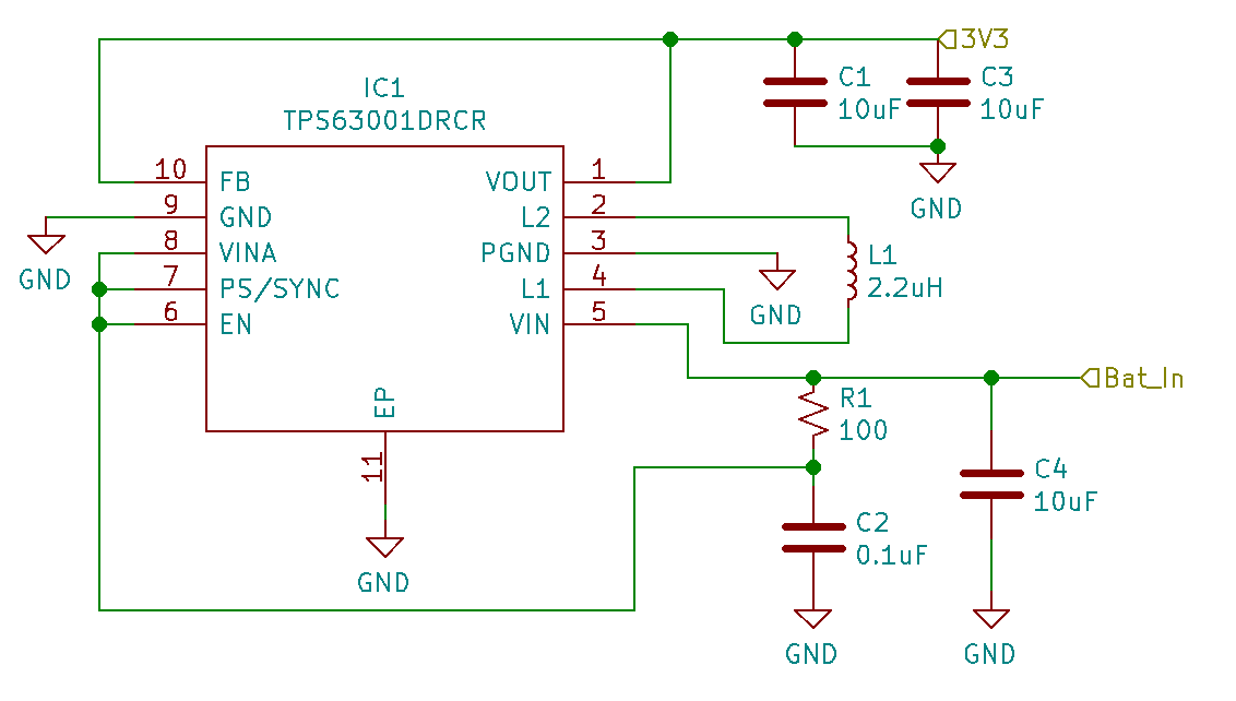
Datasheet mentions following as Quiescent current, but is this Quiescent current in case of PS/Sync kept low or in case of PS/Sync kept high?

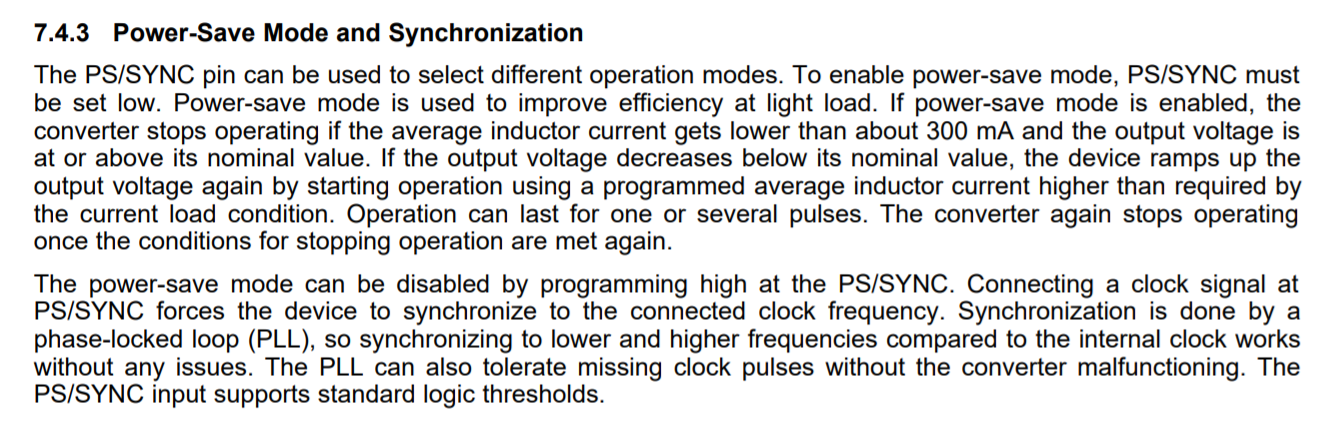
Also the datasheet mentions that if power saver mode is enabled, the converter stops operating when current goes below 300 mA, but my load is an embedded system which spends most of the time in sleep where it takes 2.3 uA, so when the converter is in power saver mode is the converter going keep powering my system or it will just stop powering the system?

Looking forward to hear from y'all!

Thanks!

Best,
Vidit Katlana

  • Hi Vidit:

    Please check the application note: https://www.ti.com.cn/litv/pdf/slyt412

    Then you will have a better understand of the Iq. 

    And the condition of converter stop switch is not with light loading, that's one of the conditions. Another is the Vout is higher than target. Usually, we do the Iq test with another DC power source and forced the Vout higher than the target.  

  • Hi Minqiu,

    Thanks for sharing the application note. It was very helpful in understanding Iq.

    From the application note, let me confirm few things first:
    1. I can confirm that measurement technique is accurate
    2. The current path is taking entire current into the IC and there is no other device involved. Only the one shown in the schematic
    3. There is absolutely no load on the VOUT of the IC

    As the application note mentions that no load current is different from Iq because even if there is no load there would still be switching of happening to compensate the leakages happening in external switches. However, this IC has all switches and MOSFETs inside the IC, is there a data on what is the no-load switching input current?

    Would like to mention that I got a better current measurement equipment and I am currently getting 1.543 mA in no-load switching input current. According to your data on IC, is that an expected current or there might be leakages on the components like inductor?

    Also the application note says that datasheet might have a graph or mention of no-load switching input current, I didn't find it yet, is there some data available on this?

    Looking to hear from you,

    Thanks!

    Best,
    Vidit Katlana

  • Hi Vidit,

    to have small no loading input current, the power save mode must be enabled. the PS pin should be logic low to enable the power save mode.