This thread has been locked.

If you have a related question, please click the "Ask a related question" button in the top right corner. The newly created question will be automatically linked to this question.

TPS386596: TPS386596, output ringing at power up

Part Number: TPS386596


Dir Sirs and Madams,


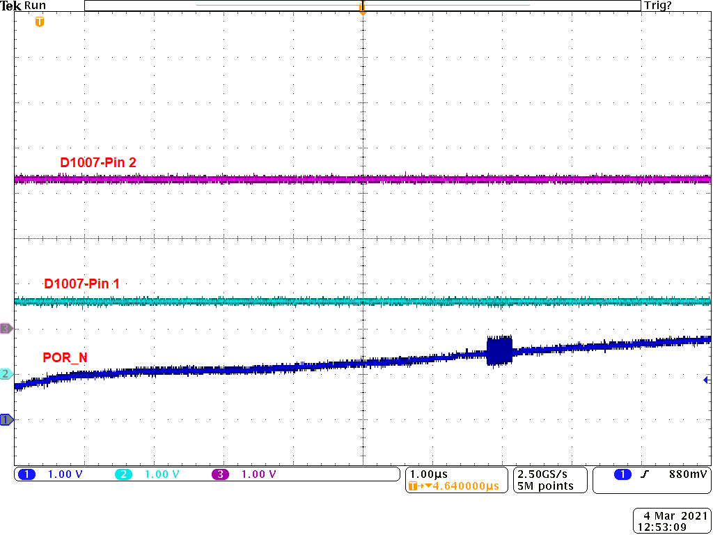
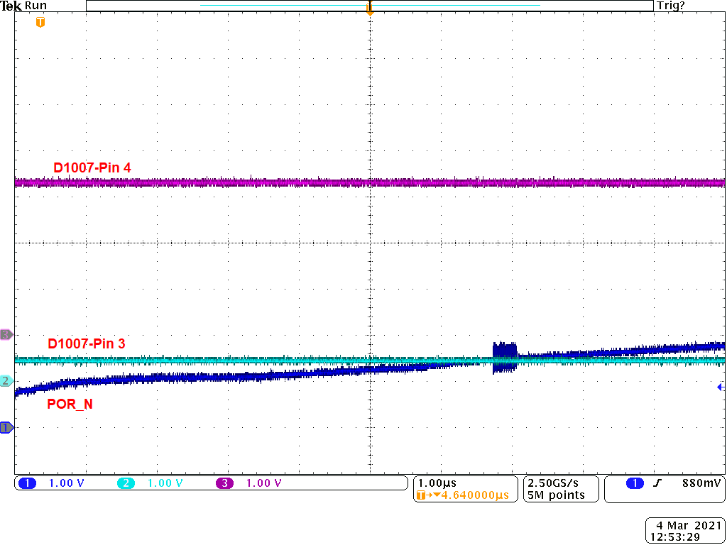
we are using TPS386596L33 as power supervisor. I have noticed some little burst at power up on output (pin 6, “POR_N”-Net) of D1007. That burst causes distortion making D1014 ringing at the output, which causes signal “FPGA_RST_N” ringing as well.

Removing output (pin 6) from net “POR_N” fixes that problem, but I also see that the voltage ramp looks different without D1007.

Adding a 10nF capacitor to the output of D1007 to GND makes a longer ringing behavior.

My questions:

  1. TPS386596L33 has an open drain output, and should not influence the voltage ramp, or am I wrong with that assumption?
  2. What do you think about that ringing (403MHz), I have done a lot of measurement, but still have no idea about the reason for behavior.


I also have done following changes to hardware, but without results:

  1. D1007: removing all MOSFET’s from D1007, decoupling all inputs with 10nF, increasing of blocking C1121, adding a LC filter to VCC of D1007, removing V1013, changing V1026 to a logic MOSFET.
  2. D1014-C: increasing of blocking C, adding a LC filter to VCC, R1180 as 10K.


Best Regards

Vitali Lach

  • Hi Vatali,

    Do you have any scope photos showing the signals going into the SENSE pins?  I am guessing that one of the signals going to the SENSE pins is noisy and causing the POR_N signal to chatter.  Is it possible to add some capacitance (0.1uF) to the SENSE pins?  

    Ben

  • Hello Ben,

    yes, I already inserted pictures with pin 1 till pin 4 from D1007, those are the sense inputs. I also have tried to add 100nF capacitor to every sense input without results. Do you think the reset output can influence the voltage ramp as an open drain output?

    Best Regard

    Vitali

  • Hi Vitali,

    No, I dont think the reset output can influence the voltage ramp as an open drain output.  Is the voltage ramp (3V3) the blue ramp signal?  What is the supply voltage to the NAND gate shown below?

    Is the supply voltage to the NAND gate have the same ramp rate as 3V3?

    If you were to remove the output POR_N from the input to the NAND gate, does POR_N still chatter?  I want to isolate the setup and take the debug one step at a time.  

    Ben

  • Hello Ben,

    thank you for helping me.

    No, it's the same voltage 3V3 for NAND supply, but not the same ramp rate. The 3V3 supply ramps long time before "POR_N" ramp, like 5V supply.

    I would add some screen shots from oscilloscope, but I’m not able to do this due to the answer limitation in this forum. I try to describe you what I have done in this case.

    I could exclude TPS386596 from this problem, detaching output of D1007 from net “POR_N” and generating Reset with some logic MOSFET V1010, I still had that ringing on  “POR_N” net. Afterwards, I have detached inputs of D1014C (74LVC02APW) and D1016C (74LVC74APW) successively from that net, without results. My colleague, who is more experienced in HF, advised me to place a RC network (50 Ohm and 10pF in series to GND) on each end of net “POR_N”, where the both “sinks” for that signal are placed . In this way we could decrease the ringing voltage to a minimum, keeping D1014 away from his threshold voltages. So we are supposing a layout issue in this case.

    Best Regards


    Vitali

  • Hi Vitali,

    It appears that you have ground bounce in the application.  That is good to know but my question is why only during startup?  My thought is that it is best to remove the output POR_N from the NAND gate and see if you are getting the "ground bounce" from the output of the TPS386596.  If you do not see the ground bounce at the output, then I would start moving towards the NAND gate.  If the output of the NAND gate is producing the ground bounce then we have determined where the ground bounce signal is coming from.  

    One thing to note, the signal that is coming from the TPS386596 is very slow, almost like an analog signal.  The input to the NAND gate should be a digital signal.  I suspect that the slow POR_N signal is causing the output of the NAND gate to chatter as the signal is passing through the transition stage.

    Ben

  • Hi Ben,

    this is also my question, why during start up. My assumption is, the net “POR_N” is a high impedance net near other FPGA signals. During start up, FPGA may produce a distortion on that net as a crosstalk effect. Following you instruction, I’ve removed the net “POR_N” from the NAND gate input. I do not see that “ground bounce” measuring directly at the output of TPS386596 (Pin 6), but if I measure the net “POR_N” near NAND gate input, I see that “ground bounce” again (its like a long end of “antenna”). This result is undependent from the GND connection point of the probes.  The ground connection is performed as a low impedance plain in the layout.

    My second question is, why the voltage ramp changes, if I detach the output of TPS386596 from the net “POR_N”. There is no problem with it, but it looks mysteriously.

    The net “POR_N” cannot be a digital signal, because of 200k pullup R1103 (now 10K), charging the gates of some MOSFET’s (V1011 and V1026) at start up. This is the reason why we see a voltage ramp on "POR_N" net.

    Best Regards.

    Vitali

  • Hi Vitali,

    That is great fine!  It seems that your POR_N trace is picking up some noise (cross-talk) from a noisy source.  This means the problem is not coming from the TPS386596.  

    Ground-bounce is caused by a weak ground where the impedance of GND is not low enough.  When a large transient current is dumped to that GND location, the ground voltage would lift above 0V.  This is what I meant by ground-bounce.

    Is the change of voltage ramp caused by the changing of the pullup resistor R1103?  Do you see the noise when you have the 10K pullup resistor?

    Ben

  • Hi Ben,

    changing of R1103 to 10K supresses that bouncing, there is some improvement with it.

    Vitali

  • Hi Vitali,

    Makes total sense.  Using a lower pullup resistor makes the total impedance of POR_N a lot less resulting in reduced voltage amplitude from the cross-talk interference.  Looking at the board layout, have you been able to isolate the switching/noisy trace that is coupling to POR_N?

    Ben 

  • Hi Vitali,

    Good luck with your application.  Glad to be of help!

    Ben

  • Hi Ben,

    thank you for helping me. I didn't isolate the noisy trace in the layout yet, but we will do a layout review for this reason.

    Best Regards.

    Vitali.

  • Hi Vitali,

    Keep me posted!  

    Ben