This thread has been locked.

If you have a related question, please click the "Ask a related question" button in the top right corner. The newly created question will be automatically linked to this question.

LM317: if the input voltage can be bigger than 40V and why Vo is limited to “37V”

Part Number: LM317
Other Parts Discussed in Thread: , MLTLDO2EVM-037

Hi team,

I am confused with the datasheet of LM317.In the first figure, we can see "In put voltage range" is up to 40V. 

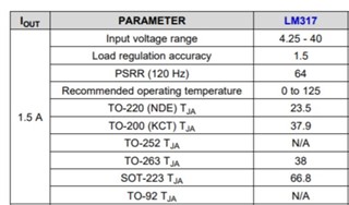
In the second figure, we can also see the "Input-to-output differential voltage max" is 40V. So I am wondering if Vinput can be larger than 40V. Is there something wrong with first "40V" for LM317 is floating?

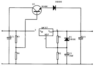
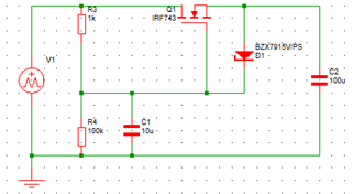
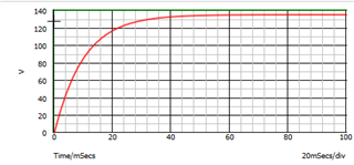
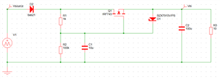
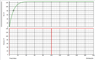
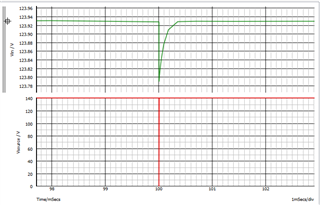
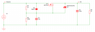
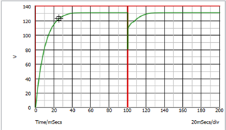
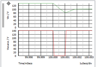
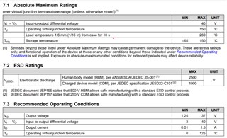
And in sheet 7.3 in figure 2. I want to figure out why Vo is limited within 37V for LM317 is floating. Are there any restrictions on Vo-Vadj?

Best regards,

Owen

  • Hi Owen,

    I think the issue is that the vast majority of linear regulators using a topology which connects Vref from the FB pin to GND.  But in a few linear regulators, like the LM317, the reference is "floating" or connected from Vout to the FB pin.  So the LM317 datasheet is using terms that are applied to most LDO's, but it can be a little confusing in this case.  It is easier to think about when you realize that the LM317 does not have a RTN pin, so these voltages are not with respect to RTN. 

    The LM317 can theoretically have 100's of voltage applied to Vin, so long as the surrounding components can withstand the voltage.  But the maximum differential voltage from Vin to Vout must not exceed 40V.  That is the requirement.  The recommended operating condition is no more than 37V from Vin to Vout because of the dropout of the device.  Modern linear regulators have dropout < 100mV, but the LM317 was designed 45 years ago.  It needs 3 volts of headroom to operate.  So if Vin = 40V then Vout = 37V maximum. 

    Examples of allowable Vin and Vout: Vin = 45V, Vout = 5V.  Vin = 200V, Vout = 160V. Vin = 10V, Vout = 7V. etc

    Thanks,

    - Stephen

  • Hi Stephen,

    Thanks for your time.

    I want to set Vin=140V,Vo=100V. The output voltage will not build quickly so that Vin-Vo will be bigger than 40V which may cause the damage of LM317. So I added Q1 to build output voltage as soon as possible to protect LM317.I wonder if the LM317 is reliable in this way. If not, how can I use it as reliable as possible.

    Best regards,

    Owen

  • Hi Owen,

    As long as you meet the abs max of the part, it should remain reliable.  But with Vin = 140V and Vout ramping slowly to charge up a large Cout, this would be a concern as you have noted.

    First, you probably should move to the high voltage version of the LM317 which can handle up to 60V.  This will give you design margin to protect your design from spurious transients and tolerances.  You can find that here: LM317HV

    You have at least two options: You can add an external transistor circuit to increase the capability of the LDO to charge up Cout.  It looks like concept is similar to what you are presenting.  Or you can add a series circuit before the LDO to slow the Vin ramp, such that the LM317 has time to charge up Cout without violating the abs max.  That concept is presented below.  You will need to change all of the values and components to suit your design, this is just the architecture for you to consider.  C2 represents the LM317 and all of its capacitance to be charged up.  R3, R4 and C1 changes the startup time.  The zener diode is selected to protect the pass FET from exceeding its abs max.

    The green waveform is the input supply turning on to 140V, and the red waveform is Vout charge up the capacitor.  This startup time changes when you modify R3, R4 and C1 as mentioned.

    Thanks,

    - Stephen

  • Hi Stephen,

    Thanks for your answer! I have one last question. If its reliable to work at Vin=140,Vo=100V? I not sure because you have given an example at Vin=200V,Vo=160V in your first answer.

    Best Regards,

    Owen

  • Hi Owen,

    If you do not exceed the 40V limitation for the lower voltage LM317, then it will not be damaged.  When you say "reliable", I think of long term operation.  The junction temperature has a significant impact on mean time before failure (MTBF), and operating at 40V differential voltage means that any current through the device will dissipate some power and raise the junction temperature. Operating at a lower differential voltage will help.  That is another advantage of the circuit I provided - you can tune Vin of the LM317 by changing the resistor divider ratio R3 and R4, which will spread the voltage drop across the Q1 pass FET and LDO.  Ultimately no real system has Vin = 140V and Vout = 100V without tolerances, so you must factor tolerance in as well into your design.

    Using the 60V rated version of the LM317 will mitigate the concerns about abs max voltage but the thermal increase on the junction will remain.  Using the circuit I provided will help you to mitigate both issues, if your system timeline can support the delayed rise on Vin to the LDO.

    Thanks,

    - Stephen

  • Hi Stephen,

    Thanks a lot for your great answer !

  • No problem Owen, let us know if you need anything else.

    Thanks,

    - Stephen

  • Hi Stephen,

    As you recommended before, the vin is delayed to LDO. But there will be another question, the Vin is delayed, which means the Vc1 will be delayed when shutting down. While at the mean time, we start Vin, and the Vin will not be delayed anymore. So the LM317 still have the potential risk when start and shut down quickly.

    Looking forward your advice.

    Owen Yan

  • Hi Owen,

    It depends on the ramp rate of the source, the duration of the brownout condition, the capacitances before and after the LM317 to hold up the voltage, and the load on the LM317 output that can discharge the capacitances.  So I'll offer some ideas for you to explore and you can let me know if you need to discuss this further.

    For these simulations I assume 100ns rise / fall times and 1us pulse width on the source supply brownout / power outage.  One option is to increase the capacitance on the input to the LDO to act as a hold up capacitor, if the brown out condition is very fast and temporary and your load is light. Since this is fairly straightforward, I did not run a simulation for this condition.

    Another option is to place a series diode in front of the circuitry to prevent the source from discharging the load switch circuitry to zero, if the power outage is fast.  Here I have a very heavy load represented by 10 ohms, but it barely makes a dent in the Vin waveform due to the fast power outage.

    Another option is to place an anti-parallel diode that is only forward biased when the source goes low, such that the C1 is discharged faster. Like this.  And you can tune the resistor divider and the capacitor accordingly.

    If I've misunderstood the question, or these options won't work for you, reply back and let me know and we can discuss further.

    Thanks,

    - Stephen

  • Hi Stephen,

    I built a circuit and did some experiments. The schematic is as below, and the load is a 1k resistance.

    I used two method to start the DC power source. The first is to use the button of DC power source, the ramp rate is slow. The second  is to use a switch to connect the circuit to the voltage established DC source, and the ramp rate is very fast. As you can see in the picture below:

    • Green: gate of MOS
    • Blue: drain of MOS
    • Yellow: Output of LM317

    In the second one, the difference between output and input of LM317HV is over 60V, for the ramp rate of DC source is too fast or the ramp rate of LM317HV output is too slow.

    I want to know how to calculate the time of LM317HV output from 0V to 100V. It's related to the output capacitor and LM317HV itself, but it's limited by LM317HV band width. Besides, the start up DC voltage is 120V, but the customer demand is 140V which may damage the LM317HV. 

    If I want to reduce the difference of LM317HV output and input, slower the ramp rate of VIN or faster the ramp rate of Vo will work, which method should I choose? 

    Thanks for your help!

  • Hey Owen,

    Can you please resend the schematic and the images, they did not come through for some reason.

    Thanks,

    - Stephen

  • Hi Stephen,

    I built a circuit and did some experiments. The schematic is as below, and the load is a 1k resistance.

    I used two method to start the DC power source. The first is to use the button of DC power source, the ramp rate is slow. The second  is to use a switch to connect the circuit to the voltage established DC source, and the ramp rate is very fast. As you can see in the picture below:

    • Green: gate of MOS
    • Blue: drain of MOS
    • Yellow: Output of LM317

    In the second one, the difference between output and input of LM317HV is over 60V, for the ramp rate of DC source is too fast or the ramp rate of LM317HV output is too slow.

    I want to know how to calculate the time of LM317HV output from 0V to 100V. It's related to the output capacitor and LM317HV itself, but it's limited by LM317HV band width. Besides, the start up DC voltage is 120V, but the customer demand is 140V which may damage the LM317HV. 

    If I want to reduce the difference of LM317HV output and input, slower the ramp rate of VIN or faster the ramp rate of Vo will work, which method should I choose? 

    Thanks for your help!

  • Hey Owen, 

    Stephen is out of office today, please give me until Thursday (4/22) to get back to you. 

    Best,

    Juliette

  • Hi Juliette,

    Thanks for reminder. Can you see the image I just resend here. Something wrong just happened that images can't be uploaded.

    B R,

    Owen Yan

  • Hi Owen,

    We can see your images now, so they are coming through to the forum.  Can you plot Vin of the LDO vs Vout?

    From a qualitative perspective, the drain of the MOSFET and the gate of the MOSFET look identical to the simulation results.  The source of the MOSFET = the input of the LDO.  It is the source of the MOSFET (or Vin of the LDO) that you will want to compare with Vout.

    Thanks,

    - Stephen

  • Hi Stephen,

    Sorry for the miss type of the blue. It is the source of MOS (Vin of LDO). 

    How to slow the ramp rate of Vin of LDO or fast the Vo of LDO. In my opinion slow the Vin of LDO might be a better way to adapt to different output capacitance.

    B R,

    Owen Yan

  • Hi Owen,

    I simulated your circuit with your components (I left out the diode across the 2.2k resistor as that should not affect this startup curve).  I see something very similar to the first curve.  It's not clear to me why LDO_Vin changes with a faster source ramp rate.  Let's start by removing the diode in your circuit across the 2.2k resistor and just measure Vin and Vgate with respect to ground. We at least know that the RC time constant formed by the 2.2k resistor, 270k resistor and 10uF capacitor will be long, like your first plot.

    The ramp rate of LDO_Vin should be dictated by the 2.2k, 270k and 10uF capacitor.  It's an RC time constant from those components which affects the voltage on the gate.  It's almost as if one of these components is not what we think it is.

    Setting the capacitor to be 10uF as shown in the schematic:

    If I change the capacitor to be 10nF, the startup is much faster (see the x-axis scale change):

    The turn on of the LM317 is limited by either (1) the current limit, Cout and Iload, or (2) the combination of Cout, Iload during turn on and the Cadj capacitor. In your case I believe it's the second one (see below).

    In the first case, if Cout is large and / or the load current is large, it will take the LM317 a long time to charge it up as the current limit is engaged around 2.2A typical.  If the Vin - Vout = 60V, then this can be 0.3A which may have an impact.  Neglecting load current (yours is light) and using the capacitor equation and the worst case 0.3A current limit: I = C*dV/dt == 0.3A = 10uF*100/dt.  Solving for dt and you get 3.33ms.  If we design the ramp for Vin such that Vin-Vout << 60V, the datasheet says the current limit will be much higher and you will not be in current limit during turn on.  So the turn on will likely be dependent on the next condition.

    In the second case, the Cadj capacitor will form an RC time constant with the parallel resistor, which will slow down Vout.  As Vout rises, most of the voltage will appear across 9.53k // 10uF in the feedback loop as only Vref is across the 120 ohm resistor.  The time constant formed by 9.53k // 10uF is approximately 100ms.  5 time constants is about 500ms.  This is basically what you are seeing in your test data.  Perhaps for now remove the Cadj capacitor until we get the waveforms working as expected, then we can add it back in later.

    Thanks,

    - Stephen

  • Hi Owen,

    To further our discussion, I tested a version of the load switch circuit as well.  The results mirror the simulations I've been providing.  In the first test I used your resistor values of 2.2k and 270k, and the capacitor in parallel with the 270k is 10uF aluminum electrolytic.  I placed a 100uF aluminum electrolytic capacitor on the output (source of the FET).  I am limited to about 50V in this test setup but the results should extend to 140V or any voltage just fine.  The MOSFET I have available is given in the link below, but the results should work for you too.  I left the diodes out as I do not need that protection in this demo setup.

    https://www.ti.com/lit/ds/symlink/csd19533kcs.pdf?ts=1619126473709&ref_url=https%253A%252F%252Fwww.google.com%252F

    One more comment - if you wish to test this on the bench, I would recommend using the MLTLDO2EVM-037 that I designed.  It was designed with 100V spacing in mind, so it is safe to at least these levels.  The other LM317 EVM's we have were not designed for high voltage spacing.  You can read the User Guide of the MLTLDO2EVM-037 for guidance on operating above 100V if you would like.

    Channel 1 = Green = Vin = 51.5V ramped in about 3ms
    Channel 2 = Purple = Vgate
    Channel 3 = Yellow = Vout

    Vin dips in the second scope shot because the 100uF output capacitor is being charged, and there is no input capacitor in the test setup.

    In the last scope shot I swapped the 10uF and 100uF capacitors so the 270k resistor is now in parallel with 100uF.  This is 10x the turn on time as expected.

    Thanks,

    - Stephen

  • Hi Stephen,

    Thanks a lot for your work!! Can I switch the 270k resistor to 2.7Mohm to achieve the same result of 100uF capacitor?

    And about the rise time of Vo(LM317), I think Cadj may help to make it faster. For a high Vo, the existence of Cadj make the voltage of adj pin slower to rise, so the resistance of LM317 is smaller. In this way, I still don't understand why the Vo of LM317 rising in a long time.

    B R,

    Owen Yan

  • Hi Owen,

    I tend to lean away from 1Meg ohm or larger resistors, as board contaminants can form a parallel resistance and impact the effective resistance.  For example, flux residue left on the board after rework can form a parallel resistance and drop the effective resistance of the 1 Meg ohm resistor.  Having said that, if your board is clean and will not be in a dirty environment in the future (industrial environments can cause dirt to collect across PCB's as well) then you should be fine with 2.7 Mohm.

    Regarding your second question on the ADJ pin - keep in mind that this is a floating reference based LDO.  So the feedback voltage is connected from Vout to ADJ.  Most LDO's have this reference tied from ADJ to GND, but that is not how the LM317 was designed.  So if you are measuring the ADJ pin with respect to ground and noticing it is slow to rise - this is the explanation on why Vout rises slowly.  The voltage from Vout to ADJ is almost immediately 1.25V, but it takes longer to raise Vout equal to the time constant of 10uF // 9.53k ohms.

    Thanks,

    - Stephen