This thread has been locked.

If you have a related question, please click the "Ask a related question" button in the top right corner. The newly created question will be automatically linked to this question.

TPS63020: Unstable output during high current consumption

Part Number: TPS63020

Hello Everyone,

I hope you are doing well.

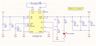
So I am using the TPS63020 as a boost converter to power an LTE/4G module. Here are the parameters:

- VIN = 3.3V

- VOUT = 3.8V

- Current consumption: Normally peaks a little over 200mA (NORMALLY!)

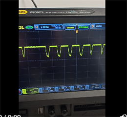
The DCDC works fine at the beginning, consumption around 20 o 30mA. But once the RF module starts searching for network, resulting in a higher current consumption, the output becomes very unstable, drops very often for very short periods of time (the red diode on PG blinks)

Also, a second anomaly is that the current consumption peaks up to 700mA which it never done before using another board and power supply.

And I have no idea why. I mostly followed the values indicated by the WEBENCH tool, so I don't really think it is an inductor problem. Maybe I am missing something in my design?

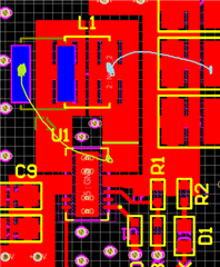
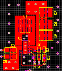
Here are the schematics and Layout:

Can someone please help?

PS: Could the value of the resistor on PGOOD be part of the problem? I see values of 100k, I only put 2.2k with mu LED on PG.

Thank you!


Best regards,

  • Hi

    1. please measure the waveform of input/output to check what happen during this period.

    2. the layout is not good. please change the layout based on the suggestion in datasheet. the IC could not behavior normally, and even damaged with bad layout

  • Hello Jasper,

    Thank you fro your answer.

    Ok I'll post the weveform as soon as I'll be back to the office.

    But for the Layout, is there anything I can do to correct the Layout on the current board?

    I guess the problem is with the output (no GND between the L and VOUT power planes). In the Layout, there is a GND plane on both TOP and BOTTOM layers (a part from the internal GND layer) that are not shown in the picture.

    Would some sort of "cage"  or one of those absorption sheets on top of the Inductor help reduce the noise?

    Can I inverse the Inductor, and link it through wires, in order to put some GND between L and VOUT like shown in the image below (in blue would be the new position of L, in green a wire to link it to the DCDC and light blue is linking the remaining plane to GND ?

    Thank you.

    Best regards,

  • Hi 

    please refer to the datasheet PCB suggestion portion to modify the PCB in the next generation.

    right now, i would suggest you apply an TPS63020EVM to check if the issue you observe is caused by the buck-boost circuit or not. 

  • Hello Jasper,

    So I have an update.

    First here is an image of how the output of the TPS63020 is during high consumption:

    The 3.9V goes down to 2.8V.

    Now here are the steps that we've done and the results we are having:

    1- We placed the Inductor further and put some GND between L and VOUT as I suggested before. This didn't change anything, not less, not mre unstability

    2- We removed te whole power supply block (DCDC and Inductor) and supplied the board directely from a Lab PS. It worked fine, even with a lot less current output (just tried to see if it  was a current supply problem)

    3- This board has a NB-IoT module, and it is stacked on another board containing the MCU and Power supply. When stacked together, the board doesn't work, as in has the same behavior as with the TPS63020. The MCU Board having also a Buck-Boost converter (not the TPS as it is an older board), and working well with another LTE/4G module, we think it is an EMI problem to which this particular module is very sensitive and causes the erratic behavior.

    4- We've ordered some shielding/absorbing sheets to put on the power supply of the MCU board and even on the bottom side of the NB-IoT board (even though there is a GND layer on the bottom of it). Maybe it will help, I'll let you know.

    Any thoughts, ideas or suggetions?

    Thank you.

    Best regards,

  • Hi 

    the voltage drop is too large, it is not normal behavior

    I would suggest to apply an EVM to check if the issue is caused by the buck-boost circuit. 

    I just notice that the input is 3.3V and output is 3.8V. so you don't need a buck-boost converter. a pure boost is better in performance and cost.

    you can apply a TPS61023EVM and connected it to your system.

  • Hello,

    You are right for the boost. I used to have an alternate power supply, thus the Buck-Boost, but then I removed it and forgot to change the DCDC (oups).

    Also, I really think it is an EMI issue.

    In the situation I discribed in point 3 in the previous answer, the 3.3V coming from the MCU board does not power the NB-IoT module anymore but only some surrounding circuits (very few), the needed 3.8V/3.9V for the module is supplied from somewhere else, which works fine when the MCU board is not connected.

    I'll see if we can get the EVM, but I don't think we will have time.

    I'll post again if we have a solution or any progress.

    Thank you for your help.

    Best regards,

  • Hi

    please also note that the circuit is sensitive to EMI if the layout is not good. always follow the suggestion in the datasheet to do the layout. DC/DC can generate noise and also sensitive to noise. 

    let me know if there is any update.