This thread has been locked.

If you have a related question, please click the "Ask a related question" button in the top right corner. The newly created question will be automatically linked to this question.

TPS61045: Abnormal output current of TPS61045

Part Number: TPS61045

Hello team,
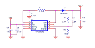
I use TPS61045 in my project, the schematic diagram as attached. My application conditions are as follows:

1. Input voltage: 4~5.5V, output voltage: 16~17V.
2. L1: 4.7uH LQH43CN4R7M03L; D1 MBR0530
3. I calculated TPS61045 can output 29mA max in my application,the actual maximum current consumption is ~15mA.
Could you help to evaluate the SCH is ok?

Recently I found that there are several IC which the output voltage is abnormal. The normal output voltage is ~16.5V and the current is ~ 10mA. The abnormal phenomena are as follows:

1. The output voltage of TPS61045 is ~20V, I measured output current is about 40mA.When I removed L1, the value of L1 changed from 4.7uH to ~0.1uH,the actual test load consumption is ~10mA. 
2. Another TPS61045 output is ~14.5V, the output current is ~15mA, I removed L1, measured L1 is 4.7uH, the actual test load consumption is ~ 8mA, where is the excess 7mA current consumption?

I have some confusion as below.

1. What are the reasons of output voltage and current of TPS61045 are so different from the theoretical calculation.
2. After I removed the inductor L1, I replaced it with a new one and the IC worked normally.The rated current of L1/4.7uH is 750mA.
Is L1/4.7uH causing the IC work abnormally or the IC causing the L1/4.7uH damage? 
3. What are the reasons that can cause the value of L1 changed?

I look forward to your analysis as soon as possible.
Thanks!

Kevin

  • Hi Kevin,

    did you see the issue in every system board? is only the inductor damaged and are two boards good after replacing the inductor

  • Hi Jasper,
    Thanks for your quick reply.

    Yes, the two boards look good.


    1. The TPS61045 outputs ~20V, the current is~ 40mA, the IC and the inductor are seriously heated, I found the abnormality and turn off the power supply. If I don't turn off the power supply, maybe the IC and the inductor will be burned. After replacing the inductor, the IC works normally, and the inductor value becomes much smaller.

    2. The TPS61045 with a current ~7mA larger than a normal IC,it has an unstable output voltage of ~14.5V, which is smaller than the theoretical value of 16.5V. Increase the load a little bit (~2mA), the output voltage will become 12V, and the chip current will increase by ~6mA. After replacing the inductor, the value of inductor is ok and the IC works normally.

    Regarding the above phenomenon, how do I need to locate the problem,could you give me some advice.

    1. For my application, is the LQH43CN4R7M03L parameter OK?

    2. If the load continues to increase, even exceeding the theoretical maximum current, how will the IC behave, and whether it will burned?

    How will the switch frequency of the IC change? Will it stop working when it exceeds 1MHz, or will it continue to work below 1MHz? What is the impact of the IC on the inductor at this time?

    Thank you for your support!
    kevin

  • Hi Kevin,

    from your description, it seem the damage of the inductor leads to abnormal of the boost circuit. from the operating principle and the current capability of the IC, such damage is unlikely caused by the IC.

    the TPS61045 is not a fixed frequency device, the frequency could be higher than 1MHz. but >1MHz frequency can't damage an inductor, which normally support > 10MHz frequency from its datasheet. 

    I don't see issue from the inductor parameter. but datasheet of the inductor is too simple, there is not much information. I would suggest you can find some support from the inductor vendor for a question such as which kind of damage happen in the inductor?

  • Hi Jasper,


    Thanks for your quick reply.

    I guess the reason for the damage of the inductor may be that the working current exceeds the rated current of the inductor.

    BTW, In the datasheet Page13,the maximum value for ILim (450 mA),
    1.What conditions of the current required by the IC will exceed 450mA?
    2.Will the IC control the maximum current(450mA)? If it exceeds 450mA, what is the working status of the IC? Will it stop working or require more current to work?


    The selected inductor must have a saturation current which meets the maximum peak current of the converter as
    calculated in Peak Current Control. Use the maximum value for ILim (450 mA) for this calculation.

    Thanks for you support.
    kevin

  • Hi Jasper,
    Thanks for your quick reply.

    I guess the reason for the damage of the inductor may be that the working current exceeds the rated current of the inductor.

    BTW,In the datasheet Page13,the maximum value for ILim (450 mA),
    1.what conditions of the current required by the IC will exceed 450mA?
    2.Will the IC control the maximum current(450mA)? If it exceeds 450mA, What is the working status of the IC? Will it stop working or require more current to work?


    The selected inductor must have a saturation current which meets the maximum peak current of the converter as
    calculated in Peak Current Control. Use the maximum value for ILim (450 mA) for this calculation.

    Thanks for you support.
    kevin

  • Hi Kevin,

    if the current is higher than 450mA, the device will stop switching, until there is short circuit in the output that make the VOUT voltage lower than VIN. but if there is short circuit, the IC would also damage.

    i was thinking if you have a failure report of the inductor to confirm the inductor is damaged by overcurrent.

  • Hi Jasper,
    Thanks for your quick reply.
    It's only my guess based on the value of inductor become smaller, I don't have a failure analysis report yet.

    I am still looking for the cause of the large current on IC.

    There are two failure which the voltage output is incorrect.
    One has a high output voltage and the IC output current is relatively large;
    The other has a low output voltage and the IC output current is slightly larger.

    What factors affect the the output voltage is far from the theoretical calculation value.
    Could you help to review my sch,the CFF is 22pF in my sch,is there any problem about 22pF,I need the output between 16~17V in my application.

    BTW, if the FB is ~0.1V,the output of IC is ~27V,is the IC damage?What is the reason for FB ~0.1V.

    Thanks for you support.
    kevin

  • Hi Kevin,

    the schematic is the same as the datasheet. I didn't see any problem. but please make sure the output effective capacitance is closed to 1uF at 17V bias condition. 

    the FB voltage is determined by the feedback resistor and VOUT if the IC is not damaged. But you said the IC is OK. could you measure the waveform of VOUT and FB to double check 27V output and 0.1V FB pin voltage behavior ?

  • Hi Jasper,

    Thanks for your quick reply.
    This is the IC for my experiment, I tested the FB impedance is  short to ground, the IC is damaged.

    I tested an IC which a slightly larger current, I tested the PIN8 of the IC,I find the main switch turn off time is ~80ns,it's turn on time is ok.
    The main switch turn off time is ~80ns,is ok? What's the minimum  turn off time of main switch.

    Could you help to analyze the reason?Is IC abnormal or inductor abnormal.

    In the page 8,the swith time minium off is 400ns,
    The main switch remains off until the minimum off time of 400 ns (typical) has passed and the feedback voltage is below the reference voltage again.

    Thanks for your support.
    kevin

  • Hi Kevin,

    for this boost circuit,  please try to change the IC, and then the inductor to double check the issue is caused by the IC or inductor. 

    if the IC is damaged, remove all the external components, then check the impedance of all the pins to GND