This thread has been locked.

If you have a related question, please click the "Ask a related question" button in the top right corner. The newly created question will be automatically linked to this question.

TPS3808G01DBVEVM: Internal Bond Wires to Circuit Supervisors

Part Number: TPS3808G01DBVEVM
Other Parts Discussed in Thread: TPS3808

Hi,

The following supervisors control the reset pin of our System on a Chip:

  • TPS3808G01DBVT
  • TPS3808G12DBVT
  • TPS3808G15DBVT
  • TPS3808G18DBVT
  • TPS3808G33DBVT
  • TPS3808G50DBVT

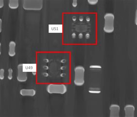
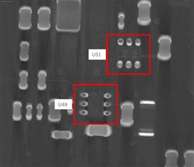
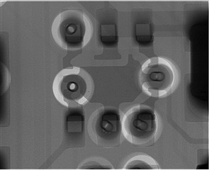
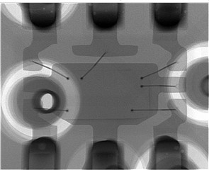
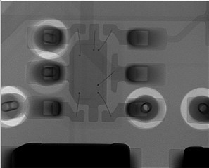
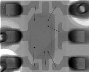
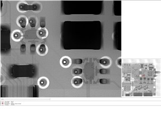
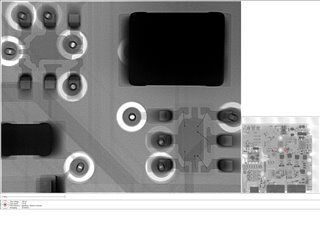
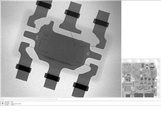
We have been having issues with our SoC powering down during a high-impact shock event on the drawer we have these supervisors installed. When x-raying the components to see if there was any damage sustained to the components or nearby traces we noticed something odd with the internal bond wires. We were able to easily make out the bond wires for the 'G12' supervisor to the 'G50' supervisor. However, the bond wires for the 'G01' were extremely difficult to see at the same magnification level as the others. We needed to zoom in much further to even barely make out the bond wires in the 'G01' I know the 'G01' is slightly different from the other supervisors since it is adjustable, however it seems odd that the bond wires would be so much thinner. Please let me know your thoughts on this.

Thanks,

Ryan Savage

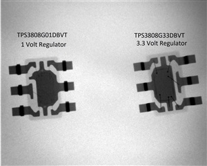
U49 is TPS3808G01DBVEVM

U51 is TPS3808G33DBVEVM

  • Hi Ryan,

    I am looking into this and I will report back if I find something regarding the bondwires.

    Other than the bondwires, are there any other questions regarding the TPS3808?

    Ben

  • Has there been any documented issues with these supervisors during a high impact shock blow? I know unlikely, but figured I would cover all my bases.

    Thanks,

    Ryan

  • Hi Ryan,

    Based from my findings, the TPS3808 and its variants are manufactured in different TI factories and all of them use the same bondwire thickness.  Therefore, the "G01" version should have the same bondwire thickness to the other TPS3808 variants you mentioned.

    Also, I don't believe there has been any documented issues with the TPS3808 during a high impact shock blow.

    Ben

  • Hi Ben,

    Thanks a lot for the info. One other question is are you aware if the bond wires may have changed to some ribbon style wire or something else along those lines? We looked at a 'G01' part from about 4 years ago and the bond wires look similar to all the rest of the supervisors. However, as mentioned above, the parts that we ordered around 2 years ago exhibit these extremely thin bond wires. Just trying to make sure we have as much information as necessary.

    Thanks,

    Ryan

  • Hi Ryan,

    The bond wires should be straight, I am not sure what you mean by ribbon style wire.  According to our assembly build sheet, both the G01 and other variants are using the same bondwire thickness.  I hope I have answered your questions.

    Ben

  • Ben,

    Thanks for the reply. I have attached some higher resolution pictures from our X-Ray machine:

    'G01': (Left bought in ~2019, right bought in ~2016) 

    'G12': (Left bought in ~2019, right bought in ~2016) 

    Orientations of IC's may be slightly off, however point trying to be made is regarding the extremely thin bond wires exhibited in the 'G01' purchased in the top left picture from 2019. Any thoughts on this?

    Thanks,

    Ryan

  • Hi Ryan,

    Thanks for the information.  I did noticed that the x-ray pics from 2019 do not have the same magnification as the pics from 2016.  Could that be the reason why the bondwires seem "so thin"?  Just curious, do you have the lot number and the date codes for the 2016 and 2019 G01 parts?

    Ben

  • The G01 and G12 pictures from 2019 were the same magnification to kind of compare the one with bonds wires to the one with barely any thickness. We couldn't find anything on the parts with lot number or date codes. Could that info possibly be underneath the part? Not a very big one to begin with.

    Thanks,

    Ryan

  • The coloration and/or focus doesnt seem to be the same.  The G12 looks more focused with more contrast.  Could it be the orientation of the part?  

    Ben

  • Yeah we kind of noticed that as well... it certainly could be. 

    Below is an image with the same magnification from the 2016 Board (U49 on left, U51 on right):

  • Any possibilities that another x-ray can be done on the G01 part?

    Ben

  • Yeah I can likely get one for Monday, but all of the newer G01 seem to demonstrate the same 'non-crisp' resolution. Saw it at the individual part level as well. 

  • Great!  Keep me posted.

    Ben

  • Ben,

    Here is another picture of U49 (G01 on the left) and U51 (G12 on the right) for the 2019 board. 

    We also performed an x-ray on the 2019 part itself and we were able to get good enough magnification to make out the bond wires quite a bit better:

    Looking into the artwork now to see if we may have added some additional copper below the part in question that could be distorting the resolution. It's just difficult to believe anything additional that was added wouldn't have affected U51 as well.

    Thanks,

    Ryan

  • Hi Ryan,

    Thanks for the additional information.  These are some awesome x-ray photos by the way.  

    Ben

  • Ben,

    This is an image comparing the 1.0V supervisor to the 3.3 V supervisor at the same magnification just laying the parts in the x-ray machine with no circuit board present. Notice how thin the bond wires are on the 1.0 compared to the 3.3.

    We are working on trying to get lot code from parts today.

    Thanks,

    Ryan 

  • Hi Ryan,

    Thanks for the photo!  Very interesting.  I will forward this information to our backend people and see what is their response.

    Ben

  • Hi Ryan,

    I think I have found your answer.  The difference between the "G01" and "G33" is the difference in bond wire material.  Certain bond wire material shows up more profoundly in the x-ray than the other material.  The materials used in the bondwires can be gold, copper, etc.  The x-ray may show that the bondwire thickness to be different between the two parts but both have the same thickness or diameter.  I hope I have answered your question.

    Ben

  • Ben, 

    Thanks a lot for digging into this. This was right in line with what our X-Ray experts in Orlando had hypothesized as well.

    Thanks again for all your help with this.

    Ryan

  • Hi Ryan,

    Glad to be of help as I also learned something new as I dug deeper into this issue.  Thanks for being patient with me.  Good luck to you!

    Ben