This thread has been locked.

If you have a related question, please click the "Ask a related question" button in the top right corner. The newly created question will be automatically linked to this question.

UCC12050: SYNC pin driven by 3.3 V signals

Part Number: UCC12050
Other Parts Discussed in Thread: UCC12040, UCC12051-Q1,

Hello, 

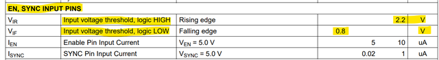
We would like to check whether the SYNC input pin can be driven with an external 3.3V clock signal, which seems feasible based on the datasheet.

Could you please confirm this?

Best regards,

Minkyun

  • Minkyun,

    Thanks for connecting through E2E. The UCC12040, UCC12050, UCC12051-Q1 SYNC pin has TTL compatible thresholds as you highlighted. Applying a 3.3 V SYNC signal is appropriate. Please pay attention to to section 7.3.5 in the UCC12050 data sheet. The applied SYNC signal must be 16 MHz ±10% and when an external SYNC signal is applied the internal spread spectrum modulation (SSM) is disabled. Without SSM active, peak EMI will be higher. Customers who prefer to drive the SYNC pin externally, as you are proposing, often use a digital clock signal that has it's own SSM (frequency dithering) capability, or they want to shift the fundamental frequency slightly away from 16 MHz. What is your goal for driving the SYNC pin externally? 

    I am supporting the application use of this device and you can contact me directly at: s-mappus@ti.com

    Regards,

    Steve M

  • Hello Steven, 

    Thank you for your quick answer. We plan to use twelve (x12) of UCC12050 to create floating 5 V sources isolated against each other. Each of them will supply a half-bridge power module. We wanted to sync all of the twelve iso dc/dc to avoid the beat issue (following the datasheet description). We selected UCC12050 for this particular capability.  

    But we did not know that the external clock signal should (or recommended to) implement spread spectrum modulation. Since the switching frequency is 16 MHz/2 = 8 MHz, we thought this is high enough in comparison with other systems' switching frequencies. For example, the half-bridge switching frequency is around 40 kHz. 

    Also, this system is for a laboratory-grade motor drive. So, we did not take EMI regulations too much into our account. Could you explain more about some risks or issues when we ignore SSM for the sync signal?

    By the way, we plan to generate the sync signal from an FPGA module. 

    Thank you for your help,

    Minkyun

  • Minkyun,

    If you are not concerned for EMI, then you also should not be concerned for "beat frequencies" and therefore, based on the use case you are describing, I would recommend not to SYNC them together or at least allow the either/or option to apply SYNC or not. You will measure some slight difference in VISO ripple between the cases of SYNC vs non-SYNC. Fanning out a 16 MHz clock to 12x points of use could potentially introduce other problems in your PCB, so be careful with your PCB layout - hopefully you can transmit these signals with good enough integrity for the SYNC at each UCC12050. Good luck with it.

    Regards,

    Steve M

  • Hello Steven,

    Thank you for sharing your opinion. It makes sense not to sync them, to be consistent in ignoring EMI issues. We plan to measure it once the prototype is fabricated. 

    As for the clock fanout - actually we were concerned about it, and eventually settled on an expensive solution: having twelve FPGA DIOs (synchronized internal to the FPGA) individually transmitting the sync signals. What would be your recommendation on a good fan-out architecture? 

    Best regards,

    Minkyun

  • Minkyun,

    I would recommend you submit that as a separate E2E thread so you can communicate with one of our digital experts. You and I are discussing power/analog issues through this thread. I will close it and you can start a new thread.

    Regards,

    Steve M