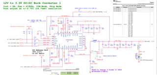
I am using repeating TPS53915 with 12V input and 3.3V output. The output is rather different from the 4 DC-DC converter.
DC-DC1 = 3.418V ;Vfb = 0.618V
DC-DC2 = 3.268V ;Vfb = 0.592V
DC-DC3 = 3.288V ;Vfb = 0.596V
DC-DC4 = 3.416V ;Vfb = 0.618V
I have add 0.1uF feedforward capacitor in parallel with upper FB resistor.
I am doing a remote sensing by connecting a thin copper from the load and route it back to the upper FB resistor.
I also have a 10ohm resistor connecting from the local 3.3V to the FB as well.
I would like to know why the output of the DC-DC1 and DC-DC4 are with 3.58% error. DC-DC2 and DC-DC3 are around 1% error which is acceptable.
Also, the Vfb reading are different as well. I thought it should be in a tight range of 597mV to 603mV.
Could you help to advise why I am seeing this problem?
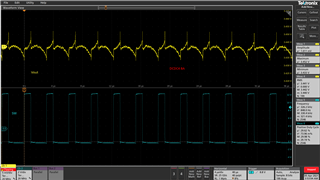
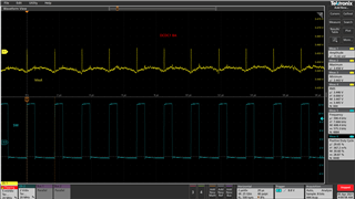
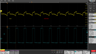
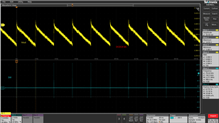
Default Fsw is 400kHz (no change of Fsw from PMBus)
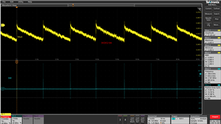
DCDC1 Cff 220pF
No Load
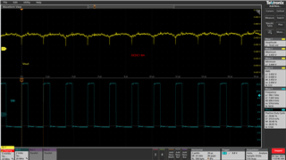
8A load
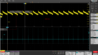
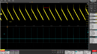
DCDC1 No Cff
No Load

8A Load
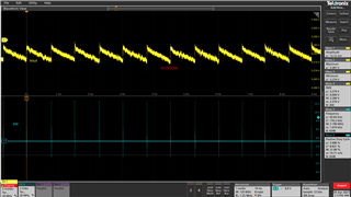
DCDC2 220pF Cff
No Load
8A Load

DCDC2 No Cff
No load
8A Load

DCDC3 220pF Cff
No Load
8A Load
DCDC4 220pF Cff
No Load
8A Load