This thread has been locked.

If you have a related question, please click the "Ask a related question" button in the top right corner. The newly created question will be automatically linked to this question.

TPS53015: Snubber & Zener circuit on SW node

Part Number: TPS53015

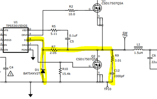
My customer is trying to reduce component count on TPS53015 design. Are both the zener + Rclamp and snubber circuit necessary on the switch node? Or is one sufficient for reducing SW node ringing - which is recommended? Our application is 12V-->3.3Vo @ 8A max

  •  

    The purpose of the snubber circuit it to reduce switch node ringing due to the parasitic inductance between the input bypass capacitance and the two power-FET.  With a good layout that minimizes the parasitic inductance and provides good high frequency bypassing, it is typically not required.

    In order to ensure good bypassing in the 50-200MHz band where switch node ringing typically occurs, you'll want to have a 2.2-10nF 0402 size bypass capacitor between the high-side and low-side FETs.  For the lowest possible inductance, place the high-side and low-side FETs on opposite sides of the PCB such that the switching node (source of high-side FET and drain of low-side FET) flow vertically through the PCB rather than in the plane of the PCB.  That will reduce switch node capacitance and parasitic inductance to help reduce ringing.

    I would not recommend removing the D1 diode circuit from the switching node.  D1 clamps the negative voltage on the SW pin, especially when the power FETs turn off during an over-current condition.  Excessive negative current beyond a few nano-seconds can establish a sub-strate current flow in the TPS53015 controller that can introduce logic errors, including errant turn-on of the high-side FET, which results in cross conduction.