This thread has been locked.

If you have a related question, please click the "Ask a related question" button in the top right corner. The newly created question will be automatically linked to this question.

UCC27212: Can't function

Part Number: UCC27212

Hello!

I have some questions about how to make UCC27212's output function as datasheet.

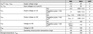
According to information on page 5, which says the maximum value for output VLO and VHO are VDD+0.3 and VHB+0.3.

datasheet page 5

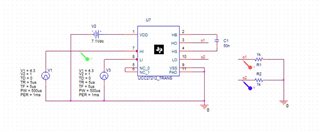
And here is my circuit and results of  simulation in Pspice, everything seems right. VLO and VHO both almost reaches VDD(7V).

simulation circuitsimulation result

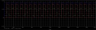
But when I test it in reality with the same circuit, I get an eccentric waveform. The next image is VLO, which is smaller than expectation obviously. VHO is nearly as same as VHS, so output of high side is close to zero. This waveform can hardly drive MOS.

input 0V-5V 50%PWM

Thanks

Auold

  • Hello Auold,

    For the HO output to operate the HB-HS bias needs to be charged from VDD through the internal boot diode. This normally occurs with a typical MOSFET half bridge configuration with the HS pin of the driver connected to the MOSFET high side source and low side drain common connection. When the low side MOSFET turns on, the HS pin switches close to ground and the HB-HS capacitor is charged from VDD through the boot diode.

    In your tested application, is the HS pin switching to ground with external MOSFET half bridge or some other path from HS to ground?  The simulation schematic does not show a connection of  HS to external power transistors. Also the LO needs to switch to allow charging of the bootstrap bias.

    Confirm if this addresses your questions, or you can post additional questions on this thread.

    Regards, 

  • Thanks for your help! Now I understand why the output of high side is about zero, because I didn't connect any circuit after the driver. The output of driver is open, so that the HS pin couldn't be close to ground and the HB-HS capacitor couldn't be charged.

    But I still have some problems about "Also the LO needs to switch to allow charging of the bootstrap bias". I'm afraid I couldn't fully understand this sentence. Is this the reason for that VLO is smaller than expectation?

  • Hello Auold,

    Thanks for confirming the understanding of the need for some connection/path on the HS pin.

    If the driver outputs are all floating, the HB cap will not be charged as you mention.

    The comment about the LO switching. In some cases even when the power MOSFETs are connected, there may still be a high resistance on the HS pin to ground if both MOSFETs are not driven. When the LO turns on, the HS switching to ground guarantees that there will be a charging path for the HB capacitor to be charged from VDD. Depending on the power train components connected to the switch node, there may be a path for the HB cap to charge, but there may not be in some cases.

    The safe way to test would be to have the power MOSFETs connected, but the high voltage not applied to the MOSFET half bridge. The low side FET switching will still charge the HB capacitor and you can inspect the driver outputs.

    Confirm if this addresses your question or you can post additional questions on this thread.

    Regards,

  • Hello Richard,

    It's so kind of you to explain the mechanism and tell me how to test safely. Please forgive my ignorance, I still have a problem about the output waveform of VLO.

    In my simulation results(picture 3), the high level of VLO(blue) is around 7V, which almost follows VDD, and the low level of VLO is around 0V. But in my experiment(picture 4), the high level of VLO is 4.635V when VDD is also 7V, and the low level of VLO is 1.435V, which is quite different from simulation.Is the situation attributed to the open circuit of driver's output? Why is the high level of the waveform so low and the low level so high?

    Thanks.

  • Hello Auold,

    Thank you for mentioning the concern about LO levels again. If the LO output is only charging the gate Qg of the MOSFET and the driver ground and low side MOSFET ground is the same, the LO should transition from close to 0 and VDD as your simulations shows. It seems there must be something loading the LO driver output or a ground shift or both.

    Can you share the actual tested hardware schematic for review? I can review to see if there is something obvious. Also check the board connections of the driver, driver to the MOSFET etc. Check the MOSFET gate to source with a DVM and see if there is some low resistance. Confirm the MOSFET source pins of the low side are connected to ground.

    If you do not want to post the schematic on the thread, you can friend me and be able to communicate in private.

    Regards,

  • Hello Auold,

    It has been a while since your last message, I assume you may have resolved the issue and will mark as such in the thread. You can always post more questions on this thread if needed.