Hello,
I would like a sanity check on my design. I bought thru hole components to prototype the buck converter but I underestimated just how small the QFN 16 package is, and unfortunately the tools at my disposal have made it difficult to ensure the IC is properly soldered to the QFN 16 - DIP breakout board (I have no access to rework station).
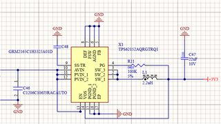
So I would like some feedback on whether my schematic is correct (ie will output 3.3V) so I can confirm that the chip is not properly soldered, because currently I get no output.
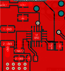
If my schematic looks good, than some feedback on my layout would be appreciated as well.