Other Parts Discussed in Thread: LM5050-2
LM5050 has leakage current of about –200μA from OUT to IN when input supply is not available or disconnected but supply bias pin VS pin is powered through OUT or external power supply.
This thread has been locked.
If you have a related question, please click the "Ask a related question" button in the top right corner. The newly created question will be automatically linked to this question.
LM5050 has leakage current of about –200μA from OUT to IN when input supply is not available or disconnected but supply bias pin VS pin is powered through OUT or external power supply.
Background:
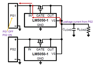
When LM5050-1 is used for ORing two are more power supply rails and one of the input supplies is removed or disconnected or not available, leakage current flows from one power supply to the other supply which is not available. Figure 1 shows ORing application of two power supply rails where PS1 is turned off or not available, leakage current flows from PS2 to PS1 through LM5050-1.

Figure 1: ORing two power supply rails using LM5050-1
This leakage current is not desirable in many applications such as battery powered rails where leakage current depletes the battery. Further, when input voltage rails are monitored using voltage supervisors or other circuit to make system level decisions such as maintenance, diagnostics, etc., presence of this leakage current path pulls the power supply rail voltage to a value higher than acceptable. This can affect the system level decisions necessary to perform maintenance or diagnostics.
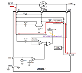
In Figure 2, the leakage current path is marked red in Functional block diagram of LM5050-1. The leakage path starts from VS bias pin connected to OUT and goes through the internal charge pump. Further when PS1 is disconnected, LM5050-1 turns of the MOSFET by internally turning ON the 2A MOSFET to short GATE to IN (Source of MOSFET), thus making VGS 0V. The 2A internal pulldown MOSFET completes the leakage current path from OUT to IN through the charge pump as indicated in Figure 2.

Figure 2: LM5050-1 Block Diagram – Leakage Current Path
Solution:
One way to solve this issue is to avoid the leakage path by connecting the VS pin either IN or other way is use LM5050-2 which does not have a separate VS pin, but the supply bias voltage is taken through IN pin.

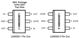
Figure 3: Pin Out Comparison LM5050-1 vs LM5050-2
LM5050-2 is easily replaceable because the only pin-out difference between LM5050-1 and LM5050-2 is pin 1 which is VS pin in LM5050-1 and nFGD FET Fault Status pin in LM5050-2. Pin Out for both LM5050-1 and LM5050-2 is shown in Figure 3. Either nFGD can be left open if not used or connected to IN/OUT through pull up resistor. Additionally this would not require PCB changes and hence recommended for designs that are close to mass production or at mass production.