This thread has been locked.

If you have a related question, please click the "Ask a related question" button in the top right corner. The newly created question will be automatically linked to this question.

TPS782: TPS78230 and TPS61222 combination circuit review

Part Number: TPS782
Other Parts Discussed in Thread: TPS61222, TPS7A03, TPS7A02

Hi, Support Team

A circuit was formed by combining the TPS78230 and TPS61222.

However, a problem has occurred, so we will contact you as follows.

First of all, please review the suitability of the configured circuit.

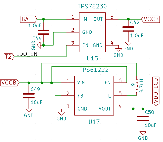
This is a problem that occurred in the circuit configured as in the circuit diagram above.

Problem 1. During PBA inspection, the TPS78230 OUTPUT LEVEL drops to 0.3V.

If C49 and C50 in the circuit diagram are removed, OUTPUT LEVEL is normally output as 3.0V.

What is causing the problem?

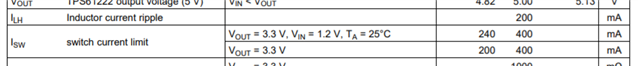
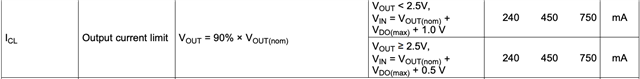
And what is the relationship between the TPS61222's IN/OUT CAPACITOR?

We will inform you of additional confirmed matters.

By separating each OUT/IN of the TPS78230 and TPS61222, it was confirmed that each output (3.0V / 5.0V) is normally output during a single test.

In case of malfunction, it has been confirmed that there is a defect and a solution to the defect according to the capacity value of C42.

C42: 1uF-defect occurred

C42: 2.2uF-defect occurred

C42: 4.7uF-Normal operation and bad operation are mixed.

C42: 10uF-normal output

Thanks.

Regards,

MJ

  • Hi MJ,

    If we need to go deeper with the boost converter, we'll need to engage the team which handles that product.  However I suspect that the LDO load current during turn on of the boost converter causes the LDO to enter current limit.  The higher values of C42 prevent this from happening by allowing C42 to provide the charge to charge up C50.  Keep in mind that during turn on, charge is transferred from Cin to Cout of any power converter (switching or linear) so typically you want Cin >> Cout to prevent any issues during turn on.  According to your tests, Cin = 2*Cout when the issues go away. 

    If you can connect a current probe between the LDO output and boost converter input, we would be able to confirm the peak current during turn on is causing the LDO to enter current limit.  You will want to measure the current, as well as Vout of the LDO, Vout of the boost converter, and Vin of the LDO to confirm it is not drooping during this event.

    Thanks,

    - Stephen

  • Hi, Stephen

    First of all, thank you for the previous answer.

    I have additional questions.

    The following is a capture of Electrical Characteristics of TPS78230 and TPS61222.

    [TPS78230]

    [TPS61222]

    It seems that the output of the TPS78230 is dropped due to the operation of the current limit. Even if you check the above spec, the current

    consumed during operation of the TPS61222 seems to exceed the capacity of the Iout of the TPS78230.

    Is this correct?

    If the above is correct, please recommend a suitable product.

    TPS61222 is Vin=3.0V, Vout=5V.

    Are there any products with low current consumption?

    Thanks.

    Regards,

    MJ

  • Hi MJ,

    Could TPS7A02/TPS7A03 possibly work here? Output current limit is as such below and seems to be 2x TPS78230

    These devices also maintain extremely low current consumption with 25nA Iq / 200nA Iq respectively.

    regards,

    Wilson