This thread has been locked.

If you have a related question, please click the "Ask a related question" button in the top right corner. The newly created question will be automatically linked to this question.

TPS549D22: TPS549D22 PMBUS issue

Part Number: TPS549D22
Other Parts Discussed in Thread: TPS546D24A

Hi Team,

My customer has PMBUS communication failure issue when using TPS549D22 (replace EM2260) with 1SG110HN2F43E2VG FPGA.

Question:

Does TPS549D22 have 8Bh register? 

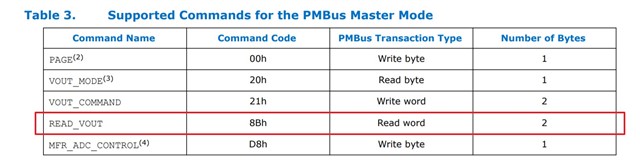
I find 8Bh in TPS546D24A but not in TPS549D22, why TPS546D24A has 8Bh but TPS549D22 doesn't have? what's the PMBUs difference between them?

The reason that I need 8Bh is because it's the power management requirement in the FPGA.

8Bh in TPS546D24A: 

8Bh in EM2260

In the Intel® Stratix® 10 Power Management User Guide, it needs to read 8Bh register. 

Best regards,

Yang

  • Hi Yang

       The TPS549D22 does not support telemetry - which means that you cannot read the VOUT, IOUT etc. from the device. 

    Thats why you dont find the READ_VOUT command here.

    Regards,

    Gerold

  • Hi Gerold,

    Does it mean that TPS549D22 cannot be used for  1SG110HN2F43E2VG FPGA

    Actually, we also tried TPS546D24A which supports telemetry. But the problem is that, the datasheet says "To ensure accurate readback,
    users must allow a minimum of 4 ms between writing a value to an individual slave and reading that same value back from the same slave."

    However, the startup timing of 1SG110HN2F43E2VG FPGA is fixed inside the FPGA with writing-reading slot is less than 4ms (user has no access to change). Hence, we also met PMBUS communication failure.

    Does it mean that TPS546D24A cannot be used for  1SG110HN2F43E2VG FPGA, either

    Or do you know which TI Device can replace EM2260 ?

    Thanks a lot.

    Best regards,

    Yang

  • Hi Yang,

    Gerold will feedback to you after the weekend. Thanks

  •  

    My apologies for the confusion, allow me to try and explain.

    First, to answer your questions:

    1) The TPS549D22 does not support READ_VOUT telemetry and can not support the external PMBus adjustment loop optional feature of the 1SG110HN2F43E2VG FPGA.

    2) While I can not speak to all of the requirements of the 1SG110HN2F43E2VG FPGA, the TPS546D24A will support VOUT_MODE, VOUT_COMMAND, and READ_VOUT, and uses ULINEAR16 format, so it should be able to support the "Master Mode" external PMBus adjustment loop feature of the 1SG110HN2F43E2VG FPGA 

    The default VOUT_MODE value is 97h, which sets the VOUT_COMMAND and READ_VOUT to Linear Format with an exponent "N" of -9, which is supported by the 1SG110HN2F43E2VG FPGA per Table 11, Page 29.  The EM2260 however uses ULINEAR16 with an exponent of -13.  To change the TPS546D24A to use an exponent of -13 you will need to update VOUT_MODE from 97h to 93h and store the updated value to NVM with the STORE_USER_ALL (Command Code 15h) command.

    The note that you are referring to in the TPS546D24A datasheet specifically refers to writing to and reading from a secondary device within a multi-phase stack of TPS546D24A devices that are sharing the current of a single output.  That is not the case for the 1SG110HN2F43E2VG FPGA VOUT_COMMAND and READ_VOUT value.

    For Example:

    If you were using 2 TPS546D24A devices to generate a single higher current output, say 0.85V at 80A, and you write a value to the second device in the stack using the PHASE Command (Command Code 04h) you need to wait upto 4ms after writing the value to the second device on in the stack before reading that same value back.

    As an example, if you wanted to adjust the READ_IOUT Offset value (IOUT_CAL_OFFSET) for the second device you would:

    1) Set the PHASE command value to 01h to address the second device in the 2-device stack

    2) Write the IOUT_CAL_OFFSET value to the new value

    3) Wait 4ms

    4) Read IOUT_CAL_OFFSET back from the second device.

    The reason for this 4ms delay is the system PMBus is not interfacing directly with the second device in the stack, it is interfacing with the first device in the stack (Phase 00h) and that device is serving as a bridge to the second device using the two-wire BCX port on the stacked TPS546D24A devices.  The first device in the stack maintains a queue of commands passing over the BCX port, but to reduce read-back latency, READ commands are given priority over WRITE commands. 

    If you write a value to PHASE 01h - 03h, and there is active communication already on the BCX bus, the write transaction will be placed in a queue to wait for the BCX bus to be available.  If you then read that same command value back before the write command has been passed to the PHASE 01h - 03h device, the READ transaction will be given priority over the WRITE transaction and the read-back will be performed before the Write and contain the wrong command value.

    The FPGA's External PMBus control loop does not use this for several reasons.

    1) It is communicating directly with Device 00h, whether that device is being used as a single device or a stack of multiple devices.

    a) It will be using PHASE = FFh (Default) or PHASE = 00h not PHASE = 01h - 03h.  Communication using PHASE = FFh and PHASE = 00h do not use the BCX "back-channel" interface and are thus not affected by any command queuing or resulting latency.

    2) It will not be reading back the same value it is writing. 

    a) It is writing to VOUT_COMMAND (Command Code 21h) and reading from READ_VOUT (Command Code 8Bh) 

  • Hi Peter,

    No need for apologize. I really appreciate your detailed analysis. 

    I will figure out how it works with customer and contact you offline. 

    thanks a lot.