This thread has been locked.

If you have a related question, please click the "Ask a related question" button in the top right corner. The newly created question will be automatically linked to this question.

BQ76200: Battery pack voltage collapses upon connecting a load

Part Number: BQ76200
Other Parts Discussed in Thread: BQ78350

Hi,

I am using the BQ76200 with the BQ78350+ BQ76200.

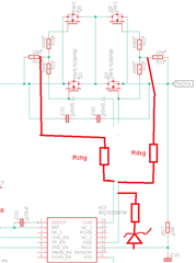
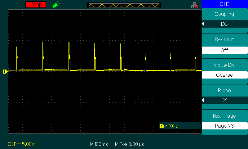
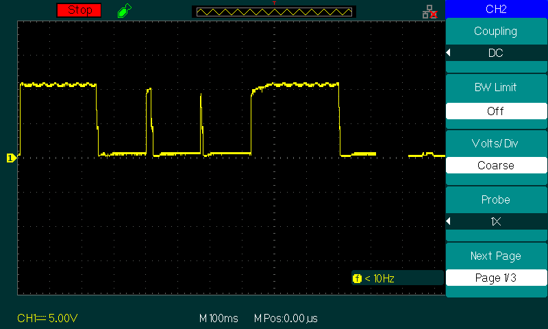
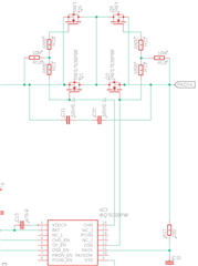
I am able to estabilish connection and turn on mosfets. I have tried testing the OCD cut-off. The cutoff happens as expected but the revival does not happen (maybe I am missing some configuration). However, after this event, post reseting the BQ78350, when the discharge is enabled and I connect the load (resistive) to the output of the system, the output voltage drops from the pack voltage to close to 0 V and the output voltage re-appears when the load is dis-connected. The partial schematic is attached for reference.

Realizing that the mosfets Q1 and Q2 don't have series resistors, I had removed the fets and performed the test.

I replaced the BQ76200 and mosfets were driven as expected. I then, retried the OCD cutoff and this resulted in the same behaviour as the last time. when the BQ76200 fails, I notice that the Vgs at the mosfet is about 1.5 V compared to 10 V when it works.

May I know if there is something I have missed and what could be the cause of this issue?

Thanks and regards

  • Hi Tarun,

    You have very capable FETs, but from the connection Q2's gate is driven directly while Q6's gate has resistance to it, so it would switch more slowly.  I don't know if your FETs may have failed by not sharing current well.  The other possibility of course is that the BQ76200 failed.  When a large current turns off quickly it can raise the voltage of the cells due to the inductive response.  I don't know your BAT voltage and if the transient approaches the maximum for the BQ76200.  BAT and PACK pins have filters, but CHG and DSG connect to the FETs and will experience transients coupled through the FETs. Another possibility might be that you have got into a state where the part is experiencing a repeated UVLO turn off and thus measures a low average gate voltage. 

    The application note www.ti.com/lit/slua794 shows a variety of information which can be helpful when designing with the part. You might check the DSG voltage when you see a low VGS to see if it is cycling similar to figures 4 or 5.  You might want a larger C13 charge pump capacitor due to the large Ciss of the FETs.

    Also check to be sure C15 is not large, 10 nF is commonly suggested, smaller can be better. 

    I would expect you might want a connection to the gates something like the following.

    The common gate resistance Rchg and Rdsg should typically be large compared to the individual gate resistances R20, R21, and R22, R23 so that both parallel FETs switch at the same time.  R20 to R23 are sometimes ferrite beads so they have low DC resistance but high frequency impedance to avoid high frequency oscillation of the parallel FETs.  You might check with your supplier to see if individual gate resistances are needed with that FET, some FETs may work fine without. 

    If your BAT voltage is high or the circuit allows the DSG rise fast enough to trigger the ESD cell as shown in the apnote, the resistor & zener between PACK and DSG pins can avoid losses and improve switching as described in the application report.

  • Thank you for that feedback.

    The Ciss of the mosfet is about 10nF and I am using only one CHG and DSG fet. So the minimum value of 470nF should be okay. Anyways, I have increased that to a 4.7nF and did the test again.

    I did probe the DSG voltage (Vgs of the DSG mosfet). At low SoC at about 10 A discharge, repeated UVLO occurs.

    Eventually, the voltage recovers as seen the image below.

    I dont suppose increasing the bootstrap caps are the solution. What can I do to fix this issue?

  • Hi Tarun,

    You did not mention if you changed the circuit topology.  See table 1 of www.ti.com/lit/slua794.  As originally drawn you have 0 ohm fro DSG to the Q2 gate.  This is likely to cycle as described in the table and your picture. IRFS7530 turns on faster than turn off, so it makes sense that it may pump up the output and eventually come on, your load might pull it down between cycles though.  If you can probe PACK+, DSG and PACK pin at the same time you can likely see what is happening during turn on.

    You likely need to add a resistor from DSG to the FET gate which allows effective turn on of the FET before the charge pump is drawn down.

    You might also check the behavior of your load.  It may have high capacitance and look like a short circuit until its voltage rises enough it can regulate and stabilize at the selected current.  You likely still have to make the circuit work with the load, but it may help to realize if you are designing to turn on into a short circuit rather than a 20A load.