This thread has been locked.

If you have a related question, please click the "Ask a related question" button in the top right corner. The newly created question will be automatically linked to this question.

ISO5852S-Q1: ISO5852S DESAT Protection variations

Part Number: ISO5852S-Q1
Other Parts Discussed in Thread: ISO5852S

Hi,

I have some doubts related to the desat protection and associated soft turn off feature in the ISO5852S gate driver.

1. Generally when someone design a gate driver using ISO5852 with high current buffer in the output then a RC circuit is connected in between Vee and OUTL pins. what is the reason of connecting this RC circuit?

2. Sometime the desat protection of the gate driver like ISO5852S is connected to the device using an Opamp instead of connecting directly with the collector or drain of the device. Can you please provide me the advantages of doing so?

Thanks,

Gaurav

  • Gaurav,

    1. Generally when someone design a gate driver using ISO5852 with high current buffer in the output then a RC circuit is connected in between Vee and OUTL pins. what is the reason of connecting this RC circuit?

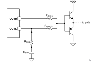
    The RC is used to tune and control the STO current when using booster.

    Because the bottom PNP is current controller, it will gain the base current (the ISO5852S STO current) to the collector current by the PNPs BETA.

    The gate of course is discharged by the IB+IC of the PNP.

    Because of the PNP current gain, we might actually end up with a larger STO current than we want. Discharging too fast can lead to VCE/VGS overshoot as a result of stray inductance, which is why STO is useful in the first place.

    That is where the RC circuit comes in (shown below). With this addition, the STO current source internal to the IC now pulls current from both the CSTO cap thru RSTO, as well as thru the normal gate drive pulldown path (thru PNP), effectively reducing the current.

    At the Point of STO, CSTO should be FULLY charged to VCC2. The RCHG / RG(OFF) ratio roughly controls how much current comes from each.

    CSTO cap store a charge of CSTO*VCC2. This way, we also have a control of the time, and can size up the CSTO cap to store more charge and thus affect STO over the full duration.

    Recommend to choose approximate values and confirm via simulation since the behavior of gate cap is not perfect like an ideal cap, for one.

    2. Sometime the desat protection of the gate driver like ISO5852S is connected to the device using an Opamp instead of connecting directly with the collector or drain of the device. Can you please provide me the advantages of doing so?

    I have not seen OPAMP used before in conjuction with the onboard DESAT detection. If it was used, i doubt it would be used for signal conditioning of the Collector/Drain, since (1) this is HV node (2) not sure what benefit it has. It would have to be isolated, AND have its own supply on the HV isolated side and its own isolated reference in order to be connected to the collector/drain.

    I could however see them using an opamp to amplify something the voltage across say a shunt resistor and in that way, provide an "Overcurrent" detection rather than DESAT by directly measuring drain/collector current. In some instances, such as for SiC, true OC detection might be preferred over DESAT which is tuned for IGBTs.

    Other parts like UCC217xx family have OC detection built in as well as DESAT variants, but using OPAMP with ISO5852S, which only have DESAT detection option, could be a way of doing Overcurrent detection, or something else.

    But OPAMP probably is not used in conjuction with a DESAT detection setup.

    The main way of changing DESAT threshold is by changing the numbers of series resistors. More series resistors, = Desat threshold is reduced by their VFs.

    You can also add series zener to increase it by the zener voltage.

    If this answers all your questions please let me know by pressing the green button.

    Best

    Dimitri

  • Dear Dimitri,

    Thanks for a detailed answer.

    The point no.1 is clear to me now.

    For point no. 2 regarding, This is not for the overcurrent protection as it does not include any shunt resistors. Does it has to do something with DC link voltage. What happens if the DC link voltage is somewhere around 2kV or 2.5kV, can we connect ISO5852S directly to the Collector or Drain of the device? Could this be the reason for using OPAMP?

    Also I feel we won't be needing any isolation if we use VDD2, VEE2 and Gnd2 for OPAMP.


    Thanks,

    Gaurav

  • Gaurav,

    2kV This is dangerously close to the max working isolation voltage rating of ISO5852S so it shouldn't be used with dc bus voltage that high.

    For DESAT detection, the collector or drain is always connected to DESAT through at least one HV blocking diode. and of course blanking cap from DESAT to GND2. This is shown in the datasheet.

    You can NOT connect the drain/collector directly to DESAT pin of the device. The chip 100% will fail on first turn on.

    Those HV blocking diodes are often rated >500V. So if you have 1kV bus you should have 3 of them to give headroom.

    For halfbridge configurations/highside driver:

    The GND2 pin for highside will float along with the switch node which will move up and down, from 0V all the way to VBUS perhaps. Everything on that driver gets referenced to this moving voltage, and VCE/VDS are never supposed to get too high when the drain is on.

    There is no need to use any opamp with integrated DESAT (unless there is some really bizarre configuration that I'm not aware of).

    I am not really sure what configuration you were thinking about using an OPAMP with DESAT but is going to interfere with the DESAT charging current. This charging current sets the blanking time via the blanking cap...

    Please see below link on DESAT circuit.

    https://www.ti.com/lit/eb/slyy169/slyy169.pdf#page=31

    If you have an example of integrated DESAT + OPAMP usage, could you please share it here?

    Best

    Dimitri