This thread has been locked.

If you have a related question, please click the "Ask a related question" button in the top right corner. The newly created question will be automatically linked to this question.

[FAQ] PCB footprint, trim/form profiles, solder dipping and reflow recommendations of ceramic space power devices

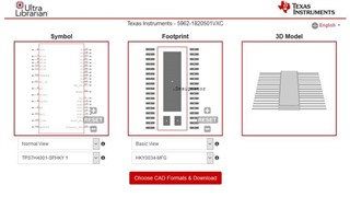
Could TI please provide guidance for how to trim/form the leads of ceramic devices and provide the PCB footprints so we can integrate into our system design?

  • The PCB footprint for ceramic devices are typically a by-product of a targeted package’s trim and form profile. Specifications on the trim and form profile vary based on the customer’s mission and board level reliability (BLR) requirements.  Texas Instruments uses the services of sub-contractors Fancort and Spirit Electronics to derive and implement the desired trim and form profiles which in turn determines the PCB footprints.  Texas Instruments does provide the PCB footprints for our ceramic packages via the respective product folders on ti.com that have been used on our ceramic based EVMs, see the below steps on how to download those files. Note these PCB footprints are provided by TI are for reference only. 


    Most of Texas Instruments’ straight lead ceramic devices have gold (Au) plated leads which protects the leads from corrosion. As solder can be brittle, we do not solder dip our straight lead ceramic packages as they have yet to go through the trim and form process. Post the trim and form process, the Au plated leads have in excess of the Industry recognized threshold level of 3% gold by weight. Leads that have higher than the 3% gold by weight can be dissolved into eutectic tin-lead solder above which the solder-joint may exhibit gold embrittlement. Thus it is recommended that gold-plated leads be pre-tinned (aka solder-dipped) before board mounting to scavenge the gold from the leads. If this is not done, there is a chance of gold-embrittlement of the board-level solder-joints. A flowing solder-pot or two passes in a static solder-pot is recommended. Also note the Solder-pot solder composition should be periodically monitored for gold content. 


    In addition, when solder reflowing ceramic devices the customer needs to be aware of the maximum temperature profiles to ensure that the solder reflow process does not damage the ceramic lid seal.  See the following link to the Texas Instruments application note on  Hermetic Package Reflow Profiles, Termination Finishes, and Lead Trim and Form.


    Accessing TI PCB  footprints is described in the instructions that follow.


    1. Access the product folder for the device of interest and click on Design & development hyperlink in top banner.

    1. Once at the Design & development section, click on the CAD/CAE symbols hyperlink in the top banner.


    1. Once at the CAD/CAE symbols section, click on the View options hyperlink in the Download column for the package of interest.


    1. The Ultra Librarian view will open as shown below. Clicking the red box labeled Choose CAD Formats & Download……


    1. …. reveals all the file formats available to download.