This thread has been locked.

If you have a related question, please click the "Ask a related question" button in the top right corner. The newly created question will be automatically linked to this question.

LM62460: OVP, tss2, Recovery From Dropout

Part Number: LM62460

Hi, I have three questions.

①I want to use LM62460 for Type-C.

When lowering the output voltage by changing the ratio of FB resistance,

the FB voltage rises and overvoltage protection works. Is this okay?

②The tss2 written in the datasheet defines the time from what to what, and how many seconds is it?

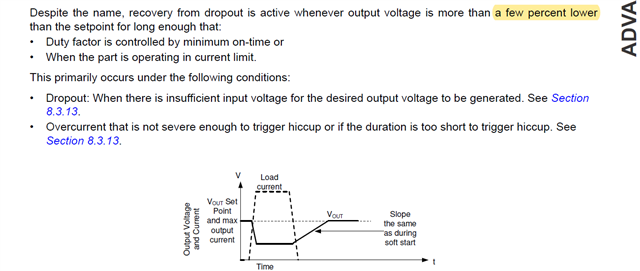
③The explanation of the Recovery from dropout function says "a few percent lower".

Specifically, what percentage drop does it take effect?

  • Hi,

    1. USB Type C applications can be easily implemented by having a fixed top resistor and have several bottom resistors and series MOSFET in parallel to control the output voltage. When you are switching in-between the MOSFETs for different output voltages (ie. 5V, 9V, 12V, etc.) the feedback voltage will try to regulate to reference of 1V. This will in turn pull the output voltage down or up depending on configuration.  How are you implementing USB Type C in your design right now? Please provide schematic for review. 
    2. I am going to check with the systems and validation team to see if there is an exact number. My guess would be to take the max specs from Ten and Tss and also add a few millisecond of delay. I've been updated by systems that you can expect a typical of 5.8ms and max of 8.4ms for Tss2.
    3. I would think that the percentage would be roughly within 2-3% of Vout.

    Regards,

    Jimmy

  • 1. I already composed the circuit like the one you explained and the image above is actual measurement waveform.
    I'm concerned that the device might be damaged because the overvoltage protection works every time the voltage is lowered.
    (I think the overvoltage protection is designed to work only in the event of an abnormality.)

    2 & 3. I understood. Thank you for your answer.

  • Hi,

    1. Can you provide the schematic of your design for me to review? 
    2. I wonder if this implementation of switching in different bottom resistors is causing issues here and spiking the feedback voltage. I was able to find some reference app note material on dynamically controllable output voltage which pairs well for USB type C applications. Perhaps you should take a look at this app note SLVA861 and implement this control method. Both top and bottom resistors are fixed and set, and a simple injection current changes the output voltage. 

    Regards,

    Jimmy 

  • Hi,

    This is part of circuit related to voltage transition.

    The above circuit is used for the DCDC for USB type-C that I've configured so far.

    If I can configure a new system, I would like to use the application you provided.

    However, this time, I need to replace only the DCDC from another company's product without changing the system, so the above circuit must be used.

    Regards,

  • Hi,

    I haven't exactly configured the EVM for USB application before so the symptoms you are seeing are new to me. 

    Does the same issue happen if you increase output voltage? (ie. 5V -> 12V).

    Regards,

    Jimmy

  • Hi,

    This symptom does not occur when the output voltage is increasing, but only when the output voltage is decreasing.

    When decreasing the output voltage, the output voltage discharge circuit is also enabled at the same time as switching the FB resistor.

    However, since it is not a powerful output voltage discharge circuit that can suppress the rise of FB voltage due to switching of FB resistance, the FB voltage rises and becomes OVP.

    When increasing the output voltage, TPS62460 oscillates to raise the output voltage, which suppresses the decrease of FB voltage due to switching of the FB resistor, so the FB voltage is maintained at 1V and does not become OVP.

    Regards,

  • Hi,

    I would suggest using the current injection (DAC) method and testing again. I wonder if the controlling of the bottom resistors through MOSFET may be introducing some noise into the FB (ie. when the voltage changes from high voltage to lower voltage the bottom resistor is instantaneously put in parallel with the other set bottom resistor). 

    When changing output voltage, the feedback pin wants to see 1V (reference) to satisfy proper output regulation and it will do whatever it can internally to get to the reference voltage. Perhaps the MOSFET control method is affecting the internal feedback loop and causing the converter's IC to momentarily raise to satisfy this 1V reference when going from a high voltage to lower voltage.

    Regards,

    Jimmy