This thread has been locked.

If you have a related question, please click the "Ask a related question" button in the top right corner. The newly created question will be automatically linked to this question.

LM5113: Class D Full Bridge Feedback

Part Number: LM5113
Other Parts Discussed in Thread: OPA455, , TLV3501

Hi, 

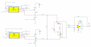
I am designing a class d full bridge amplifier with resistor load of 625m ohm and with feedback by Tina. Everything before the feedback works well. The only thing is that as I change the the resistance of my load, the feedback loop cannot correct the error. And as I change the voltage supply of my MOSFET in the power stage, the load voltage will also be changed. I follow the instruction from TI and other sources to design the circuit, but I do not know why the feedback does not work properly. Could anyone please help me solve this problem or give me some hints. Thank you so much. The schematic and program are attached. 

Best,

Tom  Test-R_load.TSC

  • Hello Tom,

    Thanks for reaching out.

    We're reviewing and will get back to you within 48hrs.

    Regards,

    -Mamadou

  • Hello Tom,

    I have reviewed your simulations and the issue appears to revolve around the feedback implementation and the OPA455.

    The gate drive section appears to switch as expected with the expected voltage on the switch node.

    I will forward to the comparators' team to help review that section of the circuit.

    Regards,

    -Mamadou

  • Hello Zehkun,

    The only Precision Amplifiers amplifier in the design is the HV OPA455 op amp. I can see that it is connected as a difference amplifier have a differential gain of 2 (1 k/ 6.5 k), or about 0.3 V/V. The inputs to the difference amplifier sense the voltage across R2, the 625 milliohm resistor which has the current being sourced and sunk through it by the two LM5113 bridge outputs. Since their output voltage and current consist of switching pulses L1, L5 and C2 form a balanced low-pass filter used to integrates the pulses and produce a dc current.

    I don't really see any problems with the difference amplifier if that is its intended purpose. The OPA455 op amp is usable with supplies up to +/-75 V, and it will work with the +/-15 V supplies being used in the circuit. The main thing when applying the OPA455 is that you remember to connect its package's underside PowerPad to the V- supply. If it is grounded, or left floating it may not function properly.

    The one item about the overall design that struck me is the difference in sources In_1 and In_2 and how they are derived. In_1 simply comes off the TLV3501 high-speed comparator push-pull output. It drives the two, opposite LM5113 inputs directly. In_2, on the other hand, uses that In_1 signal and applies it to the gate of a high-power MOSFET (IRF540). The drain of the MOSFET will follow the gate, but with a signal inversion. That is the source of In_2 and it is applied to the other two inputs of the LM5113 devices. The MOSFET has a 5 Ohm drain resistor to V+ and a lot of current flows through it as it switches states.

    If the intention is to have the In_1 and In_2 signals 180 degrees out of phase with each other, I doubt that will be the case. I expect the In-1 and In_2 signals appear quite different in their characteristics. I would connect a scope probe to each one and have a look at them. You may find there is a problem there.

    Regards, Thomas

    Precision Amplifiers Applications Engineering