This thread has been locked.

If you have a related question, please click the "Ask a related question" button in the top right corner. The newly created question will be automatically linked to this question.

TPS542941 grounding inquiry

Other Parts Discussed in Thread: TPS542941

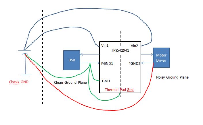
I wish to connect 2A output of the TPS542941 to clean devices (such as USB) and 3A channel more noisy devices (such as motor driver).

As such, I will need to design two different ground planes as the return path to prevent unwanted noise on clean devices. PGND1 (pin4)  will be returned to the clean ground and PGND2 (pin13) will return to noisy ground as shown in below:


Below are my inquiries:

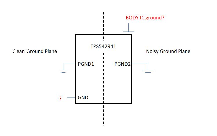
- Could you advise to which ground plane should GND (pin8) pin return to?

- I  need to return the body IC to ground as well. Can you also advise to which ground plane should the body IC return to?

  • While the PGND1 and PGND2 grounds are probably not directly shorted internal to the IC, I expect that at the IC all three grounds will need to be at the same potential.  In the datasheet, each of those pins are tied directly to GND at the thermal pad under the device.  In the datasheet example all, the ground returns from both channels are connected directly to a single ground plane with multiple vias.  I did some additional research and all of out other reference designs are done in a similar fashion.  I suppose you could make separate ground fill area for each channel, but you will still need to connect them together at the IC 9as well as the analog ground.

  • Hi John,

    Thanks for your explanation.

    Understand that IC all three grounds will need to be at the same potential. What I’m concerning is whether the noise from noisy ground plane would degrade the performance of the clean devices

    I’ve modified the diagram as below for better understanding. Could you advise if such method is feasible? Kindly advise if you have better suggestion.

  • As long as the connections that tie the separate grounds together is right at the IC, That should be acceptable ) I'll try to sketch something up later to explain).  Our design services team thinks it is may actually make things worse though.  You have to be extremely careful with leakage paths between the two grounds that create more than a single point connection.   They recommend a single common ground plane, with all returns to it tightly coupled wit multiple vias.  Also if the noise is critical on your USB side, you may want to consider a linear regulator rather than a switching supply.