This thread has been locked.

If you have a related question, please click the "Ask a related question" button in the top right corner. The newly created question will be automatically linked to this question.

LM25011 / LM25011A Operating mode

Other Parts Discussed in Thread: LM25011MY-EVAL, LM25011

Hello,

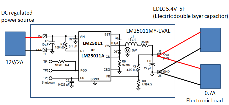
I connect electronic load and EDLC to the output of the LM25011MY-EVAL.

When the load current 0.7A in the state of EDLC is fully charged.

Load current flows from the EDLC to electric load in LM25011A.(LM25011A is stops operation)

Load current flows from the IC to electric load in LM25011.

• Input Voltage : 12V
• Output Voltage: 5.02V
• Load current : 0.7A
• Nominal Switching Frequency: 750 kHz
• EDLC(Electric double-layer capacitor) 5F/ 5.4V

Do you know the reason for the different behavior between LM25011 and LM25011A?

I want to use the EDLC as an auxiliary power source.


Best regards,
Seishin

  • Hello Seishin,

    Can you please share the schematic here. Are you trying to do a pre-bias setup with LM25011?

    Regards,

    Sourav

  • Sourav-san,

    Thank you for the response.

    The schematic is shown below.

    First to charge the EDLC after power-up, and then supplied to the load(circuit).

    When power source get blackout, EDLC can support system working by stored energy in it.

    Best regards,
    Seishin

  • Hello Seishin-san,

    If you want the EDLC to support the load you should probably use a diode between L1 and R2 Vout node (in series with R5) to prevent any back-feed from the EDLC to Vin when the DC power source is down.

    It is possible without the diode and due to the backfeed (EDLC Vout-L1-HS_FET) the was enough voltage at the Vin to keep the part up and continue to supply load. I think the diode placement should cut out the backfeed that you may be seeing.

    Regards,
    Sourav
  • Sourav-san,

    When the LM25011 in previous schematic,it will operate normally without oscillation.

    In LA25011A output will oscillate.

    When a diode is inserted between L1 and R2 Vout node, the output oscillation does not occur in LA25011A.

    What is the reason that output oscillation stops by inserting a diode.?

    Best regards,
    Seishin

  • Hello Seishin-san,

    I believe by oscillation you mean output voltage instability oscillation.

    The LM25011 and LM25011A both have a pre-charge FET inside with the idea of supporting pre-bias supply as is the case in your schematic. However, this pre-charge FET has not been characterized for this part and the functionality is not guaranteed.

    So, in the LM25011 in your circuit, it is possible the FET works as expected and helps in pulling down the SW node required to charge the BOOT cap despite the pre-bias due to the external cap and thus you do not see any issue. You will still need a diode though between the L1 and Vout for a proper pre-bias setup. However, I am not sure if this will be repeatable with other LM25011 parts.

    The LM25011A, you are using may not have a 'strong' pre-bias FET and I presume the SW node is not pulled down enough during the pre-bias and the BOOT cap discharges significantly leading to oscillations in the output. It seems this particular part will not be capable for the pre-charge bias. Hence we need to place the blocking diode between the L1 and Vout which will prevent any back-feed. in this way you are cutting out the pre-bias functionality as well.

    Hope this explanation helps.

    Regards,

    Sourav