This thread has been locked.

If you have a related question, please click the "Ask a related question" button in the top right corner. The newly created question will be automatically linked to this question.

LM3150 output 5V@10A load a resistor of 1R then the upper MOSFET broken

Other Parts Discussed in Thread: CSD18501Q5A, CSD17307Q5A

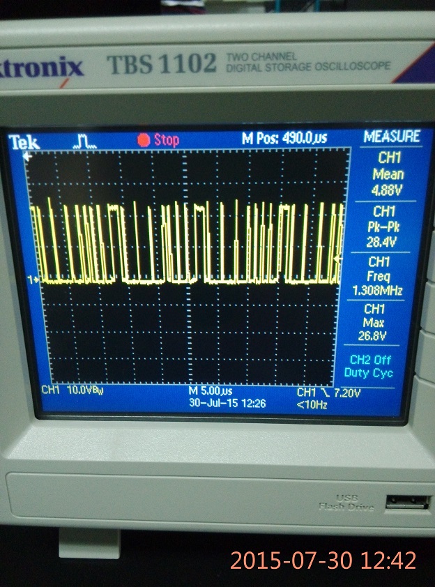
my schematic and layout as following picture, and  i don't know what cause the Q3 broken(source and drain been shorted) .

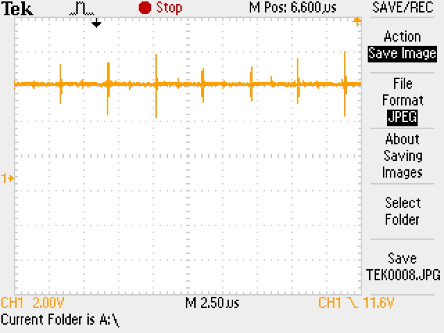
I tested the output without load , the output is 5.4V with 50mVp-p.

I added a load of 1R then after seconds I saw smoke coming out, then check the circuit and found Q3(CSD18501Q5A) was broken. 

(Other: I choose 2.2uH when design but there is only 15uH when I debug so I use it instead.)

So my question is what cause the Q3's broken and what can I do next for my 5V0@10A circuit?  Thank you for your reply.

  • Hi

    This post belongs in the non-isolated dc/dc forum. I will move it and one of my colleagues will pick it up there.

    Regards

    Peter
  • Hi,

    Can you please tell me if you are applying a fast load transient or if its a steady load being applied? Would it be possible to lower the VIN and repeat he same exercise?

    Would it also be possible to send me a snapshot of the Inductor current and gate voltage of Q3 when the load is applied?

    Thanks,

    Murray.

  • Hi Murray:

    Thanks for your reply.

    My load is cement resistor, I use 4 1R(20w) to make a larger power capacity load with paralleled two series 1R as following picture.

    I test it with lower input today, and also increase the load (change to 10R 20W cement resistor) to avoid some component broken. I test the output voltage and SW pin and take pictures, hope it means something for finding the reason.  For 24V input with 10R load , the output is a line in first seconds, and then become sawtooth. 

    If you need more information, please tell me.

    figure 1    The load when broke Q3

    Input : 24V 

    Figure2 Output with 24V in and 10R load, first seconds waveform

    Figure3 Output with 24V in and 10R load, when stable

    Figure4 SW pin signal with 24V in and 10R load when unstable

    Figure5 SW pin signal with 24V in and 10R load when stable

    Input: 12V

    Figure6 Output signal with 12V in and 10R load 

    Figure7 SW pin signal with 12V in and 10R load 

    Note:  Because of the oscilloscope's probe's GND is a little long,  so the output have many noise. I  try to short the GND line , it will be much better.

  • Hi,

    Thanks for the plots. It looks like we have some double pulsing going on. Can you let me know what the Rds(on) of Q4 is as we might not be getting enough ripple voltage generated from the Il*Rdson of the low side FET. One other thing to try would be to increase the VCC cap from 2.2uF to 4.7uF.

    Thanks,

    Murray.

  • Hi,Murray

    The PN of Q4 is CSD18501Q5A whose Rds(on) is 3.3mΩ with Vgs=4.5V and 2.5m3.3mΩ with Vgs=10V.

    Because I am back home today, I will try to increase the VCC cap tomorrow and tell you the result.

    Thanks for your attention to help me .
  • Hi Murray,

    I changed Vcc cap from 2.2uF to 4.4uF ( two 2.2uF) , the output have no change, is also a sawtooth waveform.

  • Hi,

    Sorry for the slow response I've been out of office. Would it be possible to change Q4 to a FET with a higher Rds(on) closer to 8-9mOhms? Recommendation from the calculators was SI7478DP(Vishay).

    Thanks,
    Murray.
  • Hi,

    Thanks for your reply.  I'll try the other day because I have to buy new FET first ,wish it can solve the problem.

    Thanks ,

    Laura. 

  • Hi, Murray

    I accept SI7478 today and test the circuit with SI7478 as Q4.

    Now another problem is appear , that is unstable.

    The parameters now are: C14: 4.4uF( 2*2.2uF), R6=169k, L2=SER2918H-153KL, R8=357k, c16=1500pF, c19=150pF, Q3= CSD18501Q5A, Q4=SI7478.

    Test result: (without load) : Some time the output is a stable voltage output with 5.4V; Some time the output is with triangular wave (Pk-Pk: 400mV, Period: 20us); and most of the time when I swich on the 24V in , the output is zero, or the output led flashed and then turn into zero. I need to turn on , turn off  repeat many time ,and then the output become regular output again , may with triangular wave again .

    Do you know what's wrong with it ?  Oh, i am going crazy~~~Thank you for help.

  • I know this must be frustrating, but it does seem like we are making progress.  It looks like changing the FET has made it so that the current limit is working properly and now there is no damage occurring. 

    THe instability is a separate issue and could be due to a number of factors. It would be helpful to take a single scope shot where the output ripple voltage is measured and the ripple at the FB pin is also measured.  It is possible that the the size of the feedforward resistor C19 is too large and therefore the signal at the feedback pin is too high.  Do you think you could take that measurement and share it with us?


    Thank you,

    Perry Tsao 


  • Hi, Perry

    Since i didn't receive the reply e-mail, I think there is no reply yet  and work on the other parts of my project. 

    Recent days I sent my PCB out and assemble two pcs(the old one is assembled by myself). Now I have test that , the unstatble phenomenon have disappear. I want to show you few pictures of the measurement.

    It seems that the output is also can't achieve the goal yet .   Thanks for your help .

    Figure 1: The output Without Load

    Figure2: The output with 10R Load

    Figure 3:  SW Pin with 10R Load (1)

    Figure 4:  SW Pin with 10R Load (2)

    Another proble I want to ask your help is also this kind of circuit, with design for 12V@10A . It has the same layout with my 5V@10A circuit as we talked above.

    This circuit is work like that: 

    Without load: I increase the R1 from 100k ~ 1M , the output will increase from 10V~15V. Finally I choose 499k to assemble on , and the output is about 12.5V (with about 400mVp-p). And then I add 10R load, then the output become as figure 5. 

    figure 5: 12 Output with 10R load.

  • Hi perry,

    I add the parameters as following:

    The 5V output circuit : C14: 4.4uF( 2*2.2uF), R6=169k, L2=SER2918H-153KL, R8=357k, c16=1500pF, c19=150pF, Q3= CSD18501Q5A, Q4=SI7478. ( do not change after last discuss)

    The 12V output circuit: L12:SER2918H-153KL  Q1:CSD17307Q5A  Q2=SI7478  R1: 499k  (the other  parameters are as the schematic shows )