This thread has been locked.

If you have a related question, please click the "Ask a related question" button in the top right corner. The newly created question will be automatically linked to this question.

MOSFET Drain and Source are interchangeable?-For Reverse polarity Protection

Other Parts Discussed in Thread: LM74610-Q1, SM74611

Hi,

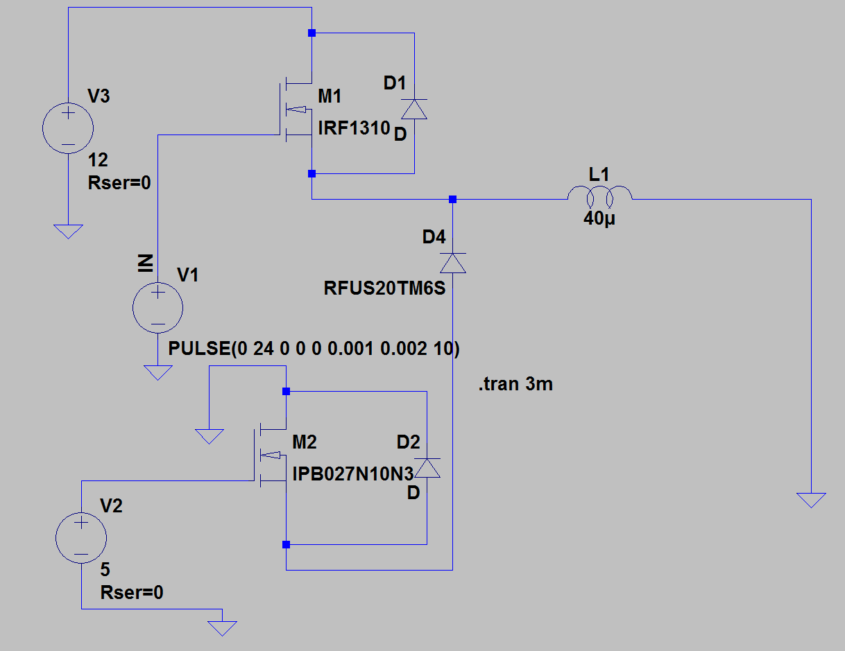
I am working with High side driver ,current of 20A (like 6 drivers) .Now I have to protect the system from  reverse voltage,since current is high I cannot connect diode in battery (+) terminal  so  I have connected the Mosfet (BUKBUK7628-100A)  the free-wheeling diode(please find the attached circuit image).
Here my question is Drain is connected to ground , source is connected to free-wheeling diode anode,and gate is connected to 5V supply always,now the MOSFET will work or not?if this is not right method please suggest some circuit.

Later i realized the n channel mosfet is fabricated on p type substrate and source and drain are (n type) sandwiched on P type substrate, Mosfet to conduct more gate voltage is needed  w.r.t  source .if  I apply  gate voltage w.r.t to drain(zero Volt) the channel cannot be formed is my understanding right.?
  • HI Bhupathi,

    It looks like you are trying to protect your end system from reverse polarity (i.e voltage and current) using MOSFETs to avoid diode forward conduction losses. There is multiple ways you can avoid Schottky diodes for reverse polarity protection. P Channel MOSFET is more traditional way in the industry, since it does not require higher GATE drive to turn on the source to drain channel. Nevertheless, there are many disadvantages of using PFET such as slow turn off response, bigger packages and higher cost. 

    N-Channel MOSFETs can be extremely effective in reverse polarity protection. There switching losses are minimal due to smaller RDSON. In addition they are available in all kind of packages, and low cost. However, you need a charge pump device or a higher voltage to drive the GATE of the MOSFET. This increases the amount of complexity. The solution becomes extremely simple if you utilize Texas Instrument's LM74610 combined with an N-Channel MOSFET as shown in the diagram below. 

    .  

    The LM74610 provides GATE drive for the  external NFET to allow forward conduction at minimal losses. There are no external components required, besides a charge pump capacitor. In the event of reverse polarity, the GATE gets pulled down by LM74610 in less than 2usec response time. This keeps the forward conduction at minimal losses thought the FET and with reverse polarity protection.

    The LM74610 is pre-RTM device, please visit the following link to see the preview datasheet. 

    http://www.ti.com/product/lm74610-q1

    best,

  • Hi Kaisar


    This looks like a really useful device. Am I right to imagine that the LM74610 is pretty much like a SM74611 ideal diode without the NMOS and pump capacitor? (why such a large capacitor, nothing like that value integrated surely)

    Can you or your colleagues give any idea of when it is likely to be available, or at least more details? Presumably samples would be available at an earlier date. Keen to try it ASAP.

    Regards

    Mike

  • Hi Mike,
    thank you for your interest in the part. The local TI sales office should be able to help you with the exact timelines and availability of samples for the LM74610.

    Regards,
    Gaurav
  • HI Mike,

    Although there are some conceptual similarities in LM74610 and SM74611 Smart Bypass diode for Solar applications, both designs are very different in their applications. Here are the main differences that make LM74610 more effective and favorable for automotive and industrial applications:

    1. LM74610 is a controller device whereas SM74611 is a module device with integrated N-FET
    2. LM74610 is a Q grade device which makes it applicable in automotive and industrial applications
    3. LM74610 is available in VSSOP 8-pin package which is much smaller than D2PAK SM74611

    In terms of their performance, here are the main differences:

    1. LM74610 is a controller device which means the circuit designers have a lot of freedom to choose ANY N-channel MOSFET with recommenced specs. The device continuously senses the polarity from source and drain of the N-channel MOSFET. There is NO ground pin, which makes the LM74610 comparable to an ideal diode rectifier. 
    2. NO Voltage or Current Limitation: With LM74610, the designer is not limited to the integrated MOSFET specs, therefore there are no positive voltage input or drain current limitations. The LM74610 can continuously protect from a negative voltage up to -45V, thus it is recommended to use for input voltage up to +45V.  There are no Drain Current limitation. 
    3. Fast Pull-Down: Contrary to SM74611, the LM74610 has a fast Gate Pull-Down pin which turns OFF the MOSFET and blocks any reverse current in the event of negative polarity with 2usec (typical). The pull-down feature of the LM74610 discharges the Gate capacitance when it senses Anode to Cathode negative voltage of -20mV. This function limits the amount and duration of the negative current to almost insignificant (2usec). The SM74611 can not turn off the Gate. 

    Hope this explanation works for your understanding. Someone from the sales would be able to assist you regarding the samples and availability.

    Best,

  • Mike,
    The Charge pump capacitor can be changed to a smaller value. The value of the Vcap doesn't affect the duty cycle of the MOSFET conduction. The only changes the frequency of the switching between MOSFET and body diode forward conduction. When the Vcap charge level drops down to a smaller threshold level (5.1V), the body diode of the FET conducts for 2%(typical) of the time to allow the charge pump capacitor to be charged to its higher threshold level (6.2V). With a smaller cap, this switching will be more frequent by the duty cycle of MOSFET on time will remain ~98%.
    Best
  • Thank you for your helpful responses.

    So the C value could be varied if required. I guess there will be a minimum value, if only to ensure the fast pull down, which requires a decent amount of Gate capacitance drive. What level of gate drive voltage is available, as this clearly affects N MOS choice?

  • Thanks Gaurav
    I spoke to Ti Europe this a.m. but they had no more information than I had already gleaned. Apart from waiting for product alerts I am in the dark. Is there a direct sales contact you can point me to please?
    Regards, Mike
  • MIke,

    The Vgs requirement for the external MOSFET is <5V. So any 45V, MOSFET with <3V threshold voltage would be appropriate to be combined with the LM74610 in reverse polarity solution. 

    The unique thing about this solution is that it allows a wide window of MOSFET selection that fit your need. 

    Best

  • Hi Mike,
    the part is now available on www.ti.com with the full datasheet and samples available to order for the LM74610-Q1.

    regards,
    GJ
  • Thanks Gaurav

    Already got samples on order. Nice part.
    Regards
    Mike