This thread has been locked.

If you have a related question, please click the "Ask a related question" button in the top right corner. The newly created question will be automatically linked to this question.

TPS7A4901 LDO wont start.

Other Parts Discussed in Thread: TPS7A30-49EVM-567, TPS7A30

Hi Everyone.

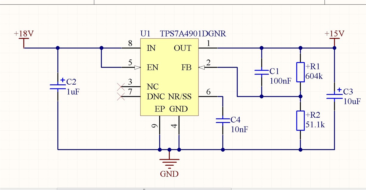
I have put together an eval circuit of the TPS7A4901, and with the exception of resistor orientation I have followed the PCB layout example of Figure 36 on page 20 of the data sheet, and the circuit diagram from Figure 9 page 12 of SLVU405.pdf (TPS7A30-49EVM-567). I set up the feedback network to give me Vout = 15V.

When I apply  ~16.5V input voltage I get nothing at the output apart from an initial jump of the output voltage from about 5 to 10 volts and then a rapid decay to ~zero. If I remove Vin from the EN pin5, then the output shoots off to ~14V, and when I reconnect Vin to EN, the output voltage settles on 15V which is exactly what I want. The TPS7A30-49EVM-567 demo board gives the correct output voltage every time, as expected.

So why am I getting these results given my layout is as close to the recommended? is there something with this part I've missed? or something else I could do to sort it out?

Thanks for your help

Martin.

SLVU405

  • Hi Martin,

    Have you tried this on multiple boards with your layout?

    Also, could you take the part from your board and put it on the EVM and the part from the EVM and put it on your board? This would let us know if the behavior is the device or the layout.

    I know you described your layout already, but If you provide a snipit of your layout around the LDO, I would be happy to give it a double check.

    Very Respectfully,
    Ryan
  • Hi Ryan, thanks for getting back to me.

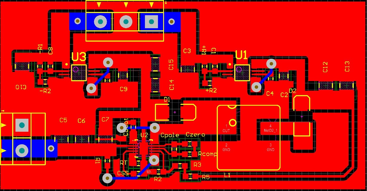
    Unfortunately I don't have the recourses to swap the chips over, but I can provide you with images of my layout, which is part of a project. Also Ryan I have looked at a couple of TI's designs and came across TIDA-0040, tidrfj9.pdf, and this doc shows a type of power good enable mechanism hooked up, not sure what its function is. Is this to fix a similar issue?

    Martin

  • Hi Martin,

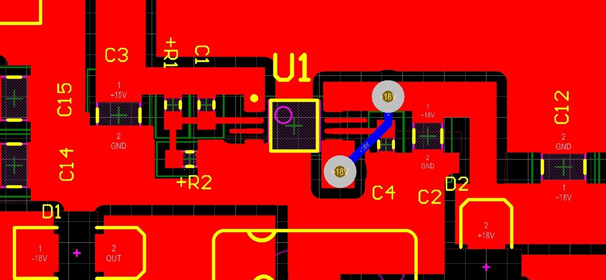
    Thank you for the layout snipits. I do not see anything that would cause your issue; however, we would recommend pouring GND under the device for the PowerPad to enhance thermal performance. Also I notice that you appear to have some leads on DNC and NC that while not connected to anything could act like antennas. Again these are suggestions, but unlikely to be the cause of your issue.

    I am not familiar with the TI design that you are mentioning and there may be a typo in your name as I was not able to locate it. Could you place a link in your next post? From your description though, adding a power good to an upstream device to trigger enable would help with sequencing; however, I do not see this affecting your application from my understanding of it.

    Is U3 in your design TPS7A30? If this is a negative rail, we have seen where some loads require the positive rail to come up before the negative rail in order for the positive rail to come up properly. It looks like you may be able to disconnect the load from the LDOs. Does your issue present without the load as well?

    Very Respectfully,
    Ryan

  • Hi Ryan.

    here is a link: www.ti.com/.../TIDA-00401

    I got to it from the link within this file: tidua78a.pdf

    tidua78a_user-guide.pdf

    The problem exists with or without load (~50mA). Thermal pad was left unconnected in this application, but its not the first PCB, the first board did have the power pad connected, with the same results. At the moment I only have the positive regulator installed.

    Martin.

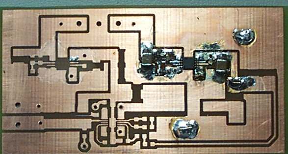
  • Ryan, I've included a pic of the PCB I have made, not the best photo quality I know.. Its not fully populated as yet, not until I solve why this LDO is not starting properly. Hope it clears up the design. The large solder blobs that are visible is where I connect Vin power.

    Martin.

  • Hi Martin,

    The enable circuitry in the TI-Design is being used for sequencing purposes.

    Thank you for the picture of your board. Due to the bare copper, your board is subject to leakage through flux. An unintended leakage path could easily cause the behavior you are experiencing.

    Very Respectfully,
    Ryan
  • Hi Ryan.

    Your last comments on the flux being a contributor made me get out the alcohol, and brush, and after a lengthy and thorough clean the behavior of the regulator did not change. I inserted an RC delay connected to EN, (100n/1M), and that allowed the LDO to start (not always reliably), but I discovered if Vin was interrupted for even a couple of 100mS, the LDO’s voltage output would drop to about 7V and not recover until Vin was removed and the delay circuit discharged completely. I can’t see what I have done that’s so different from the EVAL board to cause this. If a solution is not obvious are you able to recommend other LDO’s I could use with greater success? Also if I swapped out the 100n for a 10n, the LDO did not start at all.

    Thanks

    Martin.


  • Hi Martin,

    It looks like from the photo that the CNR capacitor is going from the NR pin (pin 6) to VIN instead of to ground, as seen in the layout.  This would create a dangerous voltage on the NR node because that node can be pulled all the way up to VIN when VIN is first connected.  Can you turn the cap. around, and swap out the part to see if that fixes it?

    Best Regards,

    Mike

  • OhNo,,,,, horrible tasteless humble pie. Can't thank you enough Mike for taking a closer look, God knows I though I had. Swapping the cap around did the trick, it appears so far the LDO still works, but I have another to swap out as soon as I get the right tools. I'm so glad you guys are there to help out.

    cheers
    Martin.
  • Ha, well the only reason I thought to look was because I've done the same myself... Hopefully it works now, let us know if anything else comes up.

    Best Regards,

    Mike