This thread has been locked.

If you have a related question, please click the "Ask a related question" button in the top right corner. The newly created question will be automatically linked to this question.

Buck Converter calculation

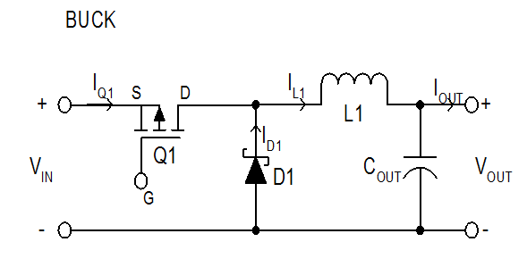
Hi all , I am trying to design a Buck converter using a tool provided by TI "http://www.ti.com/tool/buck-convcalc" the only problem is that in the excel file there is a circuit diagram (shown below) and the diagram does not have input or output capacitor banks but values are being calculated for them (E-61 and E-76) (there is a Cout and a separate field in the excel file is calculating that E-58). I can assume that the Cin bank just go at the input between the Mosfet source and Gnd and the output bank is just  in parallel with Cout but I need to be sure! any ideas?

  • let me see if I can find out who authored that tool.

  • I think those figures on the right side are just generic non synchronous buck topology and associated ideal waveforms. They are probably copied form some presentation. That spreadsheet was generated over 10 years ago, so it may be hard to track down the original. The Cin bank would go from Vin to GND. E-61 and E-76 are user inputs not calculate values. E-58 is calculating minimum output capacitance only based on steady state ripple voltage. In practice that is not the most stringent criteria for minimum output capacitance (usually load step transient response). This spreadsheet is really not a design tool. It just helps you to calculate some of the circuit parameters without having to manually calculate them, more like a basic power stage design checker, and does not work with synchronous conversion, or do anything with loop compensation, soft start, etc or any other device specific calculations

    What is your application? You are probably better served using an on line tool such as webench.
  • Hi John, Thank you for your response. Actually we need the circuit for basic science research (magnetic fields etc.) we have a 24 VDC source with 30A max current and we need to reduce the voltage to something around 0.1 volts (idealistically we want to have multiple channel of 0.1 volts that can provide 30A of current) efficiency of the circuit is not that important because our main research is not about the circuit but we need it as a tool for our main research(the simpler and easier to build the better)
  • You will find that somewhat difficult with a modern integrated solution.  Typically the internal reference voltage is between about 0.5 V to 1.25 V.  Generally that represents the lowest value output voltage.  You will have to use a controller and probably an external reference and error amplifier.  Even with a low switching frequency of say 100 kHz  (very low by modern standards), the required on time is 33.3 nsec.  That is much lower than the typical minimum on time, around 75 to 150 nsec, for most buck converters.