This thread has been locked.

If you have a related question, please click the "Ask a related question" button in the top right corner. The newly created question will be automatically linked to this question.

TPS65642 Line Transient

Other Parts Discussed in Thread: TPS65642, USB2ANY, TPS65100

Hi all,

My customer is using TPS65642 for LCD notebook panel. The MP is getting close so it's very urgent.

Input voltage is 5V and when STV signal goes high, the frame starts and input voltage (5V) makes a small dip and AVDD and GAMMA voltages also make dips.

So the color of first several horizontal lines make different color. Input capacitance is about 40uF.

What can I check to solve this problem?

Best regards,

  • Hello Sean,

    Can you monitor the input current? Please share if possible scope plot of input current with VIN, STVIN and AVDD as well.
    When does the STV signal goes high? How long are tSS2 and DLY1?

    Best regards,
    Diaara
  • Hi Diaara,

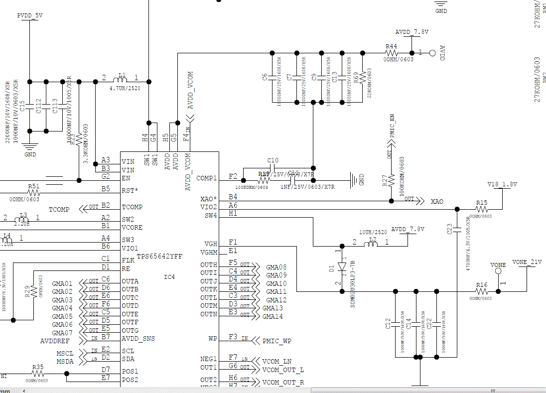
    Actually tSS2 and DLY1 don't matter because it's not happening at power-up but every frame. So all voltages are already up and AVDD drops about 300mV when STV goes high in every frame. Here's the schematic of AVDD part.

    The RC values in compensation network are 100kohm and 1nF and the datasheet says these values are recommended when Fsw = 1200kHz. But the switching frequency they're using is 750kHz so I changed the values to 56kohm and 1.5nF as the datasheet recommends. 

    After this change, the problem's gone but my customer is still wondering if this is the best way to solve this problem.

    Please let me know if you have more ideas or better solution. And let me know if you need more information to check.

    Best regards,

  • Hello Sean,

    The start of a frame is seen as a load step on AVDD. If the compensation of the AVDD converter is not optimized for the used frequency, the step response of this load step could cause visible effects on the screen. So changing the compensation network when there is a visible effect on the screen that is caused by the load step response on AVDD is the right way to solve this problem.

    If the customer wants to exactly understand what is happening and why the problem is solved when you change the compensation network, we can try to give a more detailed answer, but therefore we would need measurements of AVDD at the moment when the problem occurs before you changed the compensation and after you changed the compensation.

    Best regards,
    Brigitte

  • Hi Brigitte,

    Thanks for your reply. I asked my customer to capture scope plots and send them to me. I'll share with you once I get them.

    And my customer wants to change the switching frequency and test it but doesn't know how to change the register values. Also, I haven't supported this device before so I don't know either. Do you have a GUI for this device? Can I use USB2ANY to use the GUI and change the register values like other devices?

    And please let me know how to find optimized resistor and capacitor values. My customer wants to test many different component values to find out the optimized point.

    Best regards,

  • Hello Sean,

    The device is programmable through the I2C interface and the registers adresses and descriptions are given in the datasheet (from page 39).

     Regarding the optimization of the compensation network, I would suggest to:
    - start with the values recommended in the datasheet
    - then use the procedure described in the TPS65100 datasheet section "Converter Loop Design and Stability" (from page 16) for fine-tuning.

    Best regards,
    Diaara