This thread has been locked.

If you have a related question, please click the "Ask a related question" button in the top right corner. The newly created question will be automatically linked to this question.

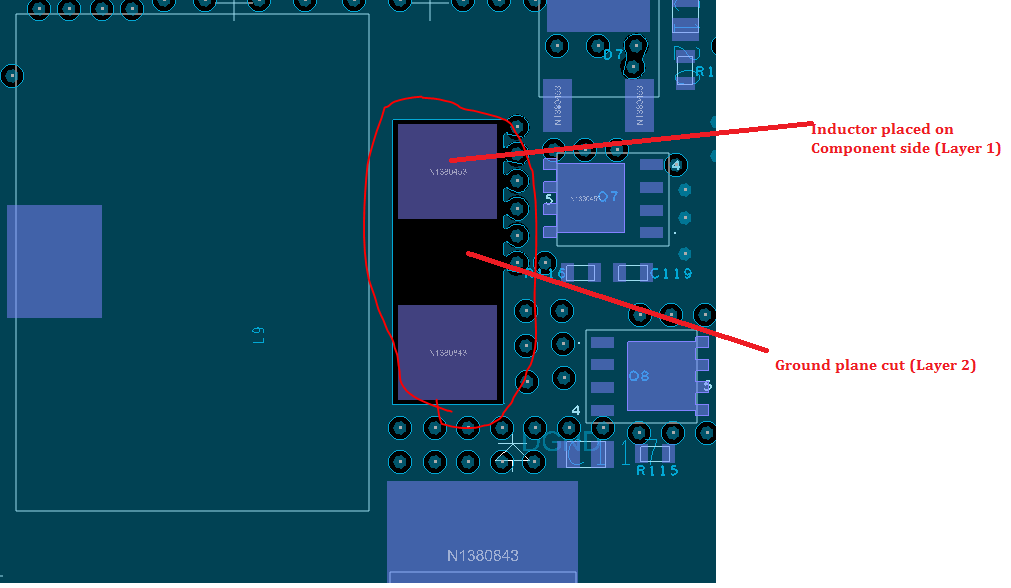
[DC/DC Converter]: Ground plane cut below power inductor

Dear All,

We are following practice of ground plane cut below power inductor used in DC/DC converter to avoid EMI issues.

The reason behind this is to avoid coupling of field with ground plane and induced noise voltages in ground plane.

But there are some different opinions which also seems logical that any cut or slot in ground plane could act as antenna because they disturb current return path.

Does anybody have explanation of which practice we should follow and when?

Thanks in advance for your help.

-Bipin

  • I typically will not place any top side copper between the inductor pads under the component.  On internal or bottom layers, I will pour a full plane under the inductor.  Just my preference.

  • Most of the indcutors used in the DCDC converters now are shielded inductors (you can check this from the inductor datasheet or its manufacture), the leakage is very very small. So you needn't take the induced eddy current in the ground plane into account.

    So Its OK to use an integraed GND plane on Layer 2. cut a slot is not a good idea.

  • Thanks John & Helen,
    So we now understand that for shielded inductors it is better to use full plane under inductor and remove any copper directly below inductor.
    However,what decision should be made when inductor is semi-shielded or not shielded?
    Sometimes from our experience we see that even shielded inductors are not that shielded.
    What is the best trade-off in this situation?
  • It has been a long time since I have used an unshielded inductor. If you want to be safe, I suppose you can cut the GND plane out on all layers (and not run any other traces under the inductor as well).