This thread has been locked.

If you have a related question, please click the "Ask a related question" button in the top right corner. The newly created question will be automatically linked to this question.

TPS62173: Reg Output to GND showing short in TPS62173 IC for USB charging in lantern

Part Number: TPS62173

Dear All,

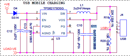
one of my customer using TPS62173 IC in LED Lantern for  USB charging and output is 5V,0.5A, they are facing issues in field and there is short showing btw Output & GND, they made about 1000 boards and facing issues in 50 boards.

USB charging schematics attached for kind reference, please help to advise your valuable feedback, thanks.

Rgds,

Aravind.

  • Hi Aravind,

    would you please provide oscilloscope waveforms of :

    • SW pin voltage
    • inductor current

    Would it be possible to send layout in pdf form?

    When is start of production?

    What is QTY for this project?

    Regards

    Lubomir

  • Hi Lubomir

    please see the attached waveform for SW Pin voltage in a working board. In the failure board since the IC is burnt and cracked we cannot get any waveforms.

    Layout in PDF form i will send.

    this product is already in production and purchased 6000 no's expected quantity 30k

  • Hi Aravind,

    • it seems that customer is using electrolytic capacitor on the input of TPS62173 with voltage rating 100V.
    • Why there is cap with so high voltage rating?
    • Is there really electrolytic cap on the input?
    • input voltage during ON time of the high side MOSFET decays, would it be possible to use input ceramic capacitor 10uF/25V/0805 and check SW pin voltage?
    • what is the input voltage range (voltage between +VE and LOAD-VE)?
    • are LEDs directly connected to J4?
    • is signal USBV used for sensing or something else?

    I am waiting for layout.

    Best regards

    Lubomir

  • Please find the answer below and attached waveform.

    1. it seems that you are using electrolytic capacitor on the input of TPS62173 with voltage rating 100V.

    We are using 2.2uF/100V at input.

    2. Why there is cap with so high voltage rating?

    Higher the voltage of the capacitor lower the ESR.

    3. Is there really electrolytic cap on the input?

    Yes.

    4. input voltage during ON time of the high side MOSFET decays, would it be possible to use input ceramic capacitor 10uF/25V/0805 and check SW pin voltage?

    Wave form attached.

    5. what is the input voltage range (voltage between +VE and LOAD-VE)?

    Input voltage can vary from 12V to 14.2V.

    6. are LEDs directly connected to J4?

    J4 is a USB connector, no LED is connected here, this is used for mobile charging.

    7. Is signal USBV used for sensing or something else?

    Yes,  used to sense the voltage of USB by the microcontroller.


    Legent Top_SOLECTRIC 120.pdf

  • Hi Aravind,

    1. as you can see from measurement SW pin voltage is not decaying during high side MOSFET on time with ceramic capacitor because of significantly lower parasitic inductance. Electrolytic capacitor has significantly higher parasitic inductance. So it is not recommended to use electrolytic capacitor as an input cap.
    2. There are recommended SMD inductors in datasheet of TPS62173. SMD inductor is smaller and allows more compact layout. There is no reason to use trough hole inductor.
    3. Smaller inductors allows to place output capacitor closer to the IC.
    4. I would recommend to follow AN for proper measuring SW pin voltage:
    5. Please find proper passive components in EVM documentation and datasheet:
    6. Will be possible to check SW pin voltage with compact layout and proper components?

    Regards

    Lubomir

  • HI lubomir

    Will this causes the failure of IC. If yes what are the reasons.

    can you please gives us more reasons for this failure.

    regards

    ramkumar

  • Hi Ramkumar,

    Voltage over-stress on the SW pin due to bad layout and wrong component selection can lead to such a behavior/failure. (Extra parasitic inductance between the input capacitor’s terminals, both power and ground, and the IC’s PVIN and PGND terminals creates excessive voltage spikes due to the switching action from V = L × dI/dt. This can lead to IC failure.)

    The input capacitor is the most important component for reliable operation of any step-down converter.

    Component selection: Please use a ceramic capacitor ⋝ 10uF as recommended in the DS. 

    Layout: Place the input capacitor as close to the IC as possible, minimizing the distance between the capacitor ground pad and the IC ground pad, as well as minimizing the distance between the input voltage connections of the two. Please follow our layout guidelines in the DS page 23.

    Best Regards,

    Michael