This thread has been locked.

If you have a related question, please click the "Ask a related question" button in the top right corner. The newly created question will be automatically linked to this question.

TL494: Can the TL494 sink current to a negative voltage rail?

Part Number: TL494

Can the TL494 sink current to a negative voltage rail? I want to tie the emitter to a negative voltage rail to switch a PMOS on the collector.
More specifically is the off state holding the base of the output transistor at 0v or does the off state connect the base to the emitter?
If it is the former my desired configuration cannot turn off.

  • Hi Sam,

    Thanks for your interest in our products, I have asked one of our engineers to respond to your post. Can you also post a schematic of your circuit? A hand drawn one would be fine, pictures are easier to follow than words.

    Regards

    Peter
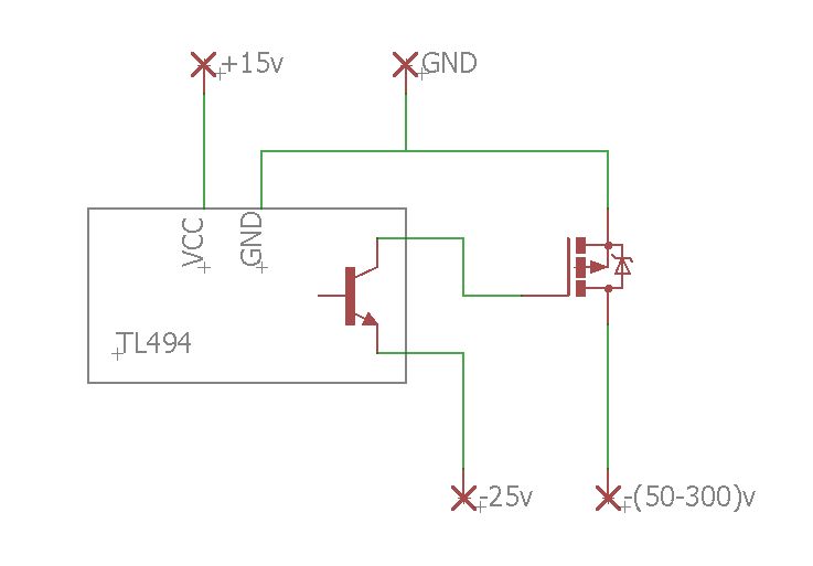
  • Here is a very basic diagram I bashed up of the desired switching method just showing the output transistor, I want to know if the output transistor will turn off successfully (and at a reasonable speed) with such a negative supply on the emitter, I can reduce the negative supply to 15v or so if need be.

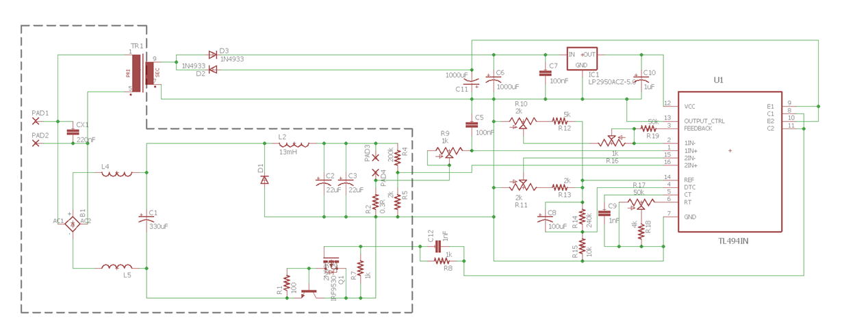
    And here is the full circuit so far, it is for driving 5-7 50W or 100W led modules in series, about 170-230v at 1.5/3.5A (output is the two pads next to the output caps).
    I have other switching methods available but I think this would be preferable.
    I couldn't find a way to use NMOS with the ground level that I need for the output feedback without using some rather dubious methods.
    I will remove the NPN transistor if I can find a PMOS to switch the full current at a reasonable price. A full BJT switch makes for a nice safe topology but I would prefer not to due to the low switching speed and needing to drain a reasonable switching current from the control circuit supply.
    It is rather experimental hence the trimmers everywhere.

  • Hi Sam,

    I have asked our IC designer to check this, will let you know once we have the answer.

    Regards,

    Bosheng

  • Thank you for the rapid support! I was thinking I might have to buy one before finishing the design just to test this.

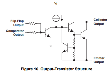
    I have done some more searching and found this diagram of the output transistor structure


    Which makes me think this a no-go since to turn off this seems to depend on the forward gate voltages of the output transistors being greater than the Vce of the inverter transistor which would not be the case with a high negative voltage on the emitter?
    I would like to hear from your designer though as I would have thought this would be noted on the datasheet if it prevented operation.

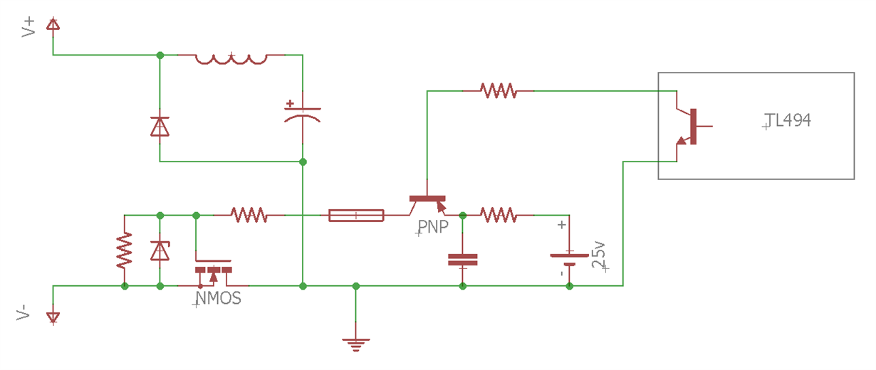
    This is my design using an NMOS switch, I feel it is not a particularly good idea though due to the fact that the pnp will be supplying the base with a voltage up to the line voltage for a short period before the mosfet turns on, the fuse is present in case it does not turn on fully to protect the zener and the rest of the switching circuit. It will also be a fair bit slower due to the high voltage BJT.
    The 25v source is from the transformer in my previous diagram, which also supplies the control circuitry.

    Do you think this a reasonable topology? Otherwise I am considering either lowering the switching speed to use a full BJT switch and just dealing with the high ripple and it's effects on the pwm control, or abandon PWM altogether by just having a simple output comparator separated from the the oscillator & switching by an optoisolator, which will require a second LV power supply and make for somewhat poor regulation but that is not a huge concern for the application.

  • Please allow some time for our IC designer to check for this.