A related question is a question created from another question. When the related question is created, it will be automatically linked to the original question.
If you have a related question, please click the "Ask a related question" button in the top right corner. The newly created question will be automatically linked to this question.
TLV62090: TLV62090 overshoot, pls advice how to improve.
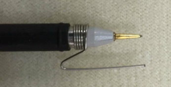
First of all, I would be sure that those measurements have been taken with the right probing technique.
I would suggest you to read the following application note: www.ti.com/.../slva494a.pdf
At point 3 it's explained how to minimise the probe insertion parasites that can cause those overshoots at the switching node.
If the problem still persists, please do not hesitate to ask further and we will solve it.
I think that what you call echo in the picture is the conduction of the low side FET's back diode during the dead time.
Dead time is the time between on-and-off phases of low and high side FETs. It is needed in order to avoid cross-conduction between the FETs, which can cause damage to the device due to high currents, or loss in efficiency when the energy (current*voltage*time) during the crossoconduction is not enough electrical-over-stress. Hence I wouldn't worry much about that "undershoot".
I would rather check what happens when the high side turns off and low side turns on! I have highlighted in green in the picture below a weird oscillation, which shows the SW node suddenly going up for a little while..this is a possible sign that the high side is being turned on again before the low side back diode starts conducting the inductor current. Indeed you can see that there is no "undershoot". That means that the current may pass directly from the high side to the low side, and as a consequence, you may have the crossconduction mentioned above.
This behaviour of double turn on of the high side is caused by both the amount drain-source capacitance and the slope of the SW node (dV/dt*C=i) which can cause a current that charges the high side gate-source cap through the drain-gate high side parasitic capacitance, eventually turning on the device.
To better understand this behavior I recommend the reading of "Modeling switching losses in MOSFETs half-bridges", G. Di Capua, N. Femia, IEEE SMACD 2012.
Back to us, the device is designed to avoid this behaviour and allow the backdiode to conduct during the dead time. Indeed I think the snubber capacitors, especially C225, which are not mentioned in our datasheet's application example, are the cause of this effect. I would chose different values and dimension them so that you can see backdiode "undershoot" in the green oval.
the Abs max voltage rating for the SW node is Vin+0.3V in DC and 10V in AC for less than 10 ns. If the device behaviour stays in these it's reliabilty will stay as expected as well. Regarding EMC rediation, I'm sorry can't give much advice.