This thread has been locked.

If you have a related question, please click the "Ask a related question" button in the top right corner. The newly created question will be automatically linked to this question.

TPS40170-Q1: Design Issue

Part Number: TPS40170-Q1
Other Parts Discussed in Thread: CSD18537NQ5A

Hi Support,

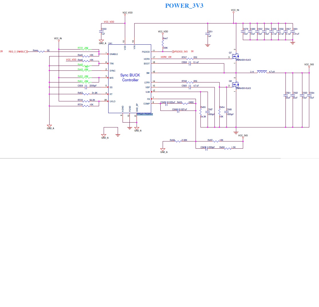
I designed the circuit of TPS40170QRGY IC dc to dc converter with the help of WEBENCH.

Our Requirement.

12V INPUT

3.3V OUTPUT

6A OUTPUT CURRENT

Here I attached the design we cant get the 3.3V output voltage. There is no shorting or no component damage.

Even I done below change and check the output but its not helpful to me.

  1. Give REG_2_ENABLE Externally.
  2. SS Pin Cap 2.2nf also check with 47nf.
  3. Check with R455 6K OR 5K.
  4. Put 0Ohm Resistance at R768 & R767 0Ohm.

Can you help me to verify the design and give some suggestion?

Here is the design

  • What does the board layout look like?

    I'd debug it by checking Vin voltage at the Vin pin, then check enable pin voltage, then check the UVLO pin voltage. Then check VBP should have LDO output voltage. If all of the above is there, please use a scope to check the LDRV output waveform and the HDRV output waveform. If the gate drives are correct (since there's no output, the duty cycle on the gate drive signal should be max duty cycle). Then please probe the waveform at SW pin.

    Hope you can locate which link is not working right.

    -Yang
  • Hi Yang,

    Thank for your valuable input. Actually we are replace this MOSFET DMNH3010LK3  with TI's CSD18537NQ5A MOSFET and the converter is working now.

    But we cant identify which parameter of MOSFET affect so that we cant get the any output.

  • Good to know!

    -Yang