This thread has been locked.

If you have a related question, please click the "Ask a related question" button in the top right corner. The newly created question will be automatically linked to this question.

LM5114: Design for LM5114B CL capacitor problem

Part Number: LM5114


Hi Sir,

As shown, the change in CL will affects the switching rise time and fall time. In the rise time is 41 ns when the CL reaches 5000 pF, For the 6.78 MHz frequency, the cycle / 2 is more than half, but in the specification CL does not make it clear where the capacitor?


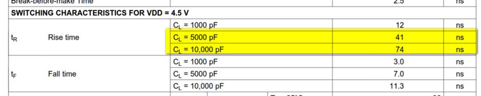
1. Could you ask where CL is? Is the output load capacitor ?

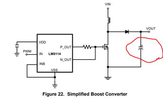
2. If yes, by the marking red circle is the output capacitor of the Boost converter. Does it affect the integrity of the output voltage waveform or ripple. Does it affect the output of the front gate driver?
3. In addition, the output capacitor of the boost converter is generally above the uF level, according to LM5114 specification CL changes 1000pF ~ 10000pF are far less than the uF level
4.Is there any risetime / fulltime equation for CL?
Thank you

Kevin

  • Hi Kevin,

    Great to hear from you!

    1. CL is meant to describe the load capacitance being driven which is the input capacitance of the power mosfet. This is typically described in the power mosfet data sheet as CISS.

    2. This is the filtering capacitor for the boost converter. It’s value does not affect the gate driver directly.

    3.  This is not applicable.

    4. The gate rise/fall time is at first order an RC time constant consisting of the input capacitance of the power mosfet, gate resistor, and output resistance of the driver.

    Let us know if you have further questions. If this answered your questions, please press the Green button to let us know.