This thread has been locked.

If you have a related question, please click the "Ask a related question" button in the top right corner. The newly created question will be automatically linked to this question.

TPS3700-Q1---How to choose an suitable value for RT

Other Parts Discussed in Thread: TPS3700-Q1, TPS3700

    Hi,

    I have some additional questions about the TPS3700-Q1:

     1.How to choose an suitable value for RT?

     According to my calculation like:

     Assumption: V(Monitor)=5V

     I(INA+ + INB-)=25+15=40n A

     RTV(Monitor)/100* I(INA+ + INB-)=5/100*40=1.25Mohm

     I am not sure if my calculation is right for RT ?

     Consider our product is not recommended for use the resistor higher than 100Kohm, so my question is if we can choose the more higher current than the input current at the INA+ and INB- terminals?……

   For example, 1500- times , thus RTV(Monitor)/1500* I(INA+ + INB-)=5/1500*40=83Kohm….Is it ok ? or Will it bring the bad influence to device?

    2.There has two equations for R2’s calculation, thus we will figure out two value…How to choose the value?


3.How to calculate the pull up resistor on the output line?

   My understanding: Rpu=(Vpu-VLV) /IS  (Vpu: Pull up voltage ;VLV: Output voltage low  ;IS: Output sink current)

   Is it right?


4.If it necessary to reserve the bypass capacitor on Input line(INA+, INB-)?


     Thanks!!!


  • Hi,

    decreasing of resistors in no problem. Datasheet also shows resistances in the 10k range. See figure 14, 18 and 20 of datasheet.

    Tell us more about your application.


    Kai

  • Hello User!

    Find the answers to your questions below.

    1. RT = R1 + R2 + R3 and should be approx. 100 times larger than the leakage current into to internal sense comparator for a good tradeoff between accuracy and power consumption. When in doubt, a RT of approx. 1 Meg ohm will work. You can reduce your resistor values less than 100k and the accuracy will improve but your Iq will be towards the higher end which is no problem.

    2. Both equations are correct, just different ways of looking at the same value. One equation looks at "the value to release the undervoltage condition when VDD is rising from "low" to above Vit-" and the other is "the value to start the undervoltage condition when VDD is falling from above Vit- to "low". This is the same thing but one is looking at the rising voltage condition and the other looks at the falling voltage condition. The only difference when changing perspective of rising VDD or falling VDD is the hysteresis. Either equation will work, just depends on how you want to look at the situation for your application.

    3. correct. Usually ~10k to ~300k should work. Always double check your output sink current is much less than max value of 40mA.

    4. The bypass caps will help prevent false triggers due to noise or supply transients. They are not required but can make your application more robust and immune to glitches.

    Please let me know if you have any other questions. Thanks!

    -Michael

  • Hi Michael,

        Thanks for your feedback!

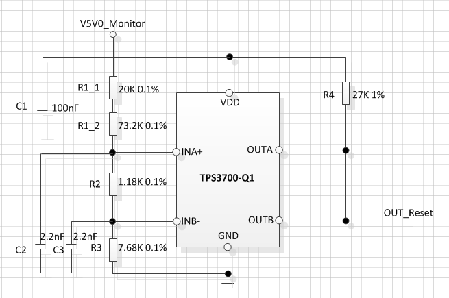
       Could you help me to double check the following circuit: ( Is it can work? )

       Our requiremnt: we need to monitor V5V0_MONITOR (V5V0_Monitor voltage range :4.9V to 5.1V)

       When V5V0_MONITOR <4.7V ,then TPS3700 should output low ;

       When V5V0_MONITOR >5.2V ,then TPS3700 should output low ;

       When 4.7<V5V0_MONITOR <5.2V ,then TPS3700 should output high ;


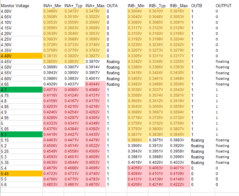
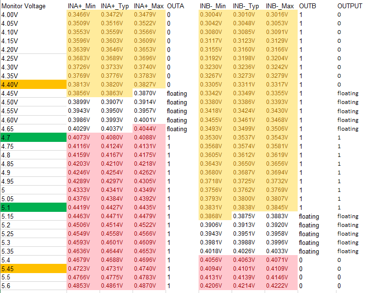
      But recently we made a short calculation about the above concept , we found there has many floating status at some voltage range. my compenstion those floating status are affected by VIT+ and VIT-. 

      You can see the below calculated picture :

      My understanging like the below for OUTA:

     when INA+ <387mV(VIT-), then OUTA output Low.

     when INA+ >404mV(VIT+), then OUTA output High.

     when 387mV <INA+<404mV, then OUTA output floating.

     My question is i don't know how to control those floating status for our design? Do you have some sugeestion?Many Thanks!!!


  • Hi Kai,
    Thanks for your reply!
    My question like I replied to Michael. Can you see the pictures in the comment?
  • Hi,

    no, I cannot see pictures in your last post, unfortunately.

    Have you mounted pull-up resistors at the outputs of the chip?

    Kai

  •   Could you help me to double check the following circuit: ( Is it can work? )

       Our requiremnt: we need to monitor V5V0_MONITOR (V5V0_Monitor voltage range :4.9V to 5.1V)

       When V5V0_MONITOR <4.7V ,then TPS3700 should output low ;

       When V5V0_MONITOR >5.2V ,then TPS3700 should output low ;

       When 4.7<V5V0_MONITOR <5.2V ,then TPS3700 should output high ;


      But recently we made a short calculation about the above concept , we found there has many floating status at some voltage range. my compenstion those floating status are affected by VIT+ and VIT-. 

      You can see the below calculated picture :

      My understanging like the below for OUTA:

     when INA+ <387mV(VIT-), then OUTA output Low.

     when INA+ >404mV(VIT+), then OUTA output High.

     when 387mV <INA+<404mV, then OUTA output floating.

     My question is i don't know how to control those floating status for our design? Do you have some sugestion?Many Thanks!!!

    Hi kail, now can you see the pictures?

  • Hi,

    There should be no case where the output is "floating".

    We have created a handy tool to help users calculate the correct resistors for any application. Please try out this tool and let me know if this helps you.

    Provide feedback if the tool does not help you.

    /cfs-file/__key/communityserver-discussions-components-files/196/8424.Supervisor-Resistor-Calc-for-TPS3700-and-TPS3701-.xlsx

    -Michael

  • Hi Michael,

        Thanks for you calculator tool! It's useful for us!

        But I have same question as I mentioned before.My question is about the accurate and output is "floating"

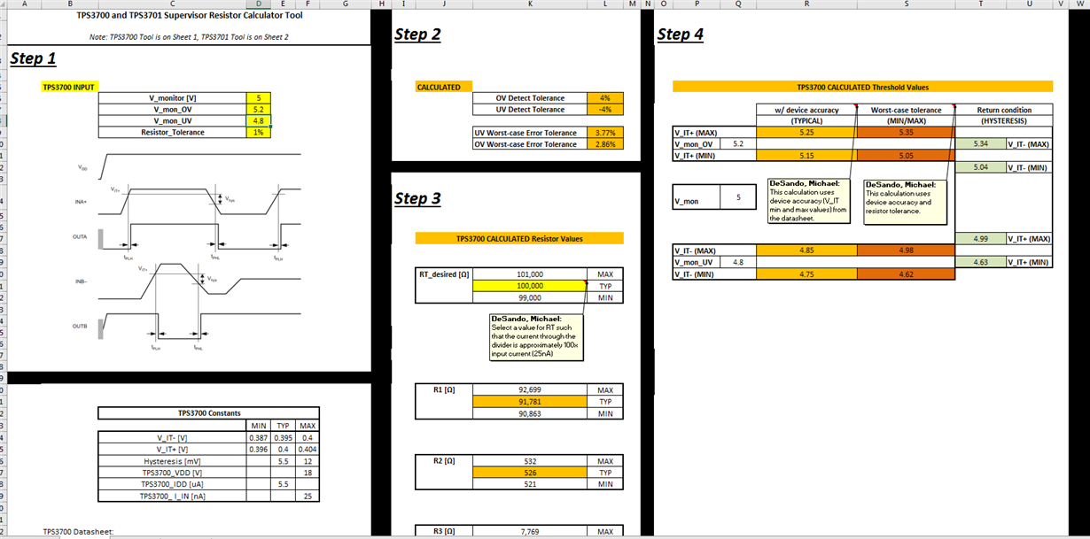
        For example: We configurated the parameter as below picture.

        OV situation:

        V_mon_OV=5.2V ; we can see V_IT+_(MAX)=5.35V and V_IT+_(MIN)=5.05V; and the return condition : V_IT-_(MAX)=5.34V and V_IT-_(MIN)=5.04V

       Normally we can ensure when V_IT+>5.35V, then OUTA output is high.  (higher than maxmium value)

       Normally we can ensure when V_IT-<5.04V, then OUTA output is low. (lower than minmium value)

       But we can not guratee the 5.04V<V_IT+<5.35V, what does OUTA output? high ,low or floating? becuase there has tolerance at device and resistors....

       I don't know whether my understanding is right?

     Thanks!

  • Hi user,

    your assumption is wrong. You wrote:

    "when INA+ <387mV(VIT-), then OUTA output Low.

    when INA+ >404mV(VIT+), then OUTA output High.

    when 387mV <INA+<404mV, then OUTA output floating."

    This is wrong! First, INA+ must go above 400mV to make OUTA going high. Afterwards, when INA+ is decreased again, OUTA stays high during INA+ is between 394.5mV and 400mV. OUTA only goes low, when INA+ goes below 394.5mV. So, there's no undefined state and there's no floating.

    Kai

  • Hi User,

    The between state you refer to is the effect of the hysteresis of the internal comparator. The output will remain in the state it is in until it passes the falling threshold for that device. The reason the device has this hysteresis is so if the supply is moving right around the detect voltage, the output will change frequently but with the added hysteresis, the supply will need to pass slightly below the rising trip voltage.

    And the worst case calculations occur only under worst case device conditions and component tolerances. The most typical conditions will occur in the middle of the min-max range.

    -Michael
  • Hi Kai,

       Thanks for your feedback! You are right !

        I had corrected it in my last post!

       Thanks!!!

  • Hi Michael,
    Thanks for your reply!
    I said the "floating" state is base on that you said the satiuation under worst case device conditions and compoment tolerances.
    Thanks!!!Wish you have nice day!!!