This thread has been locked.

If you have a related question, please click the "Ask a related question" button in the top right corner. The newly created question will be automatically linked to this question.

BQ25892: Charger startup sequence and current limitation

Part Number: BQ25892
Other Parts Discussed in Thread: TPS5420, BQSTUDIO

Hi,

I have a small design with a GSM module and I use as power management the BQ25892 chip.

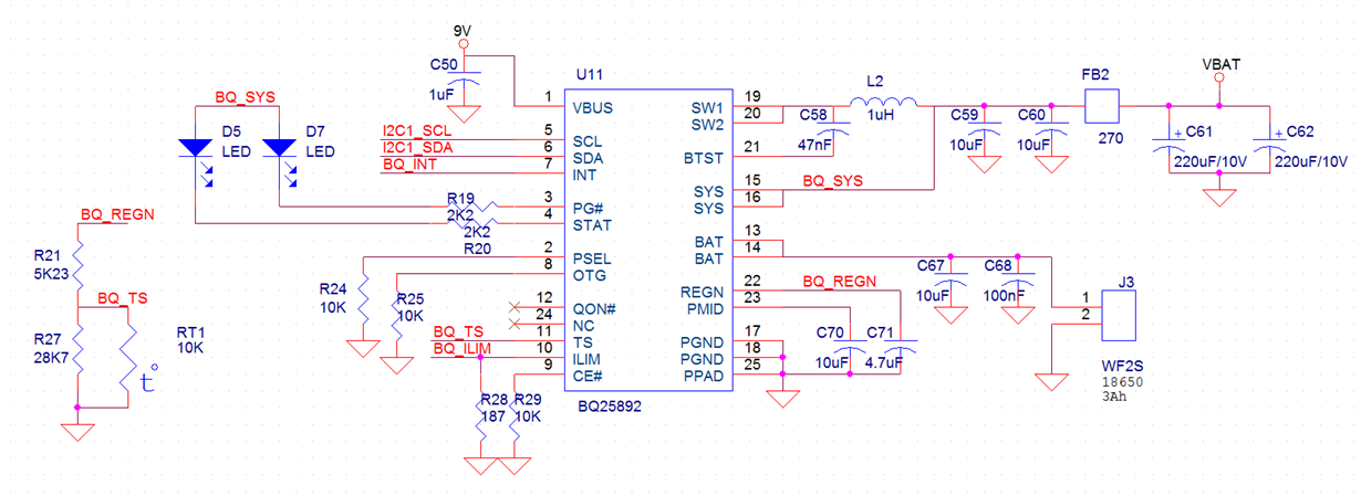
The design input voltage is regulated using a TPS5420 converter with the output set at 9V. BQ25892 is getting this 9V voltage as input voltage. The battery is a Li-ION 18650 3.7V, 3000mAh.

The GSM module is working with voltages between 3.4V and 4.4V. I need BQ25892 to have the SYS output voltage between 3.5V and 4.2V.

I'm using the following design for the battery manager:

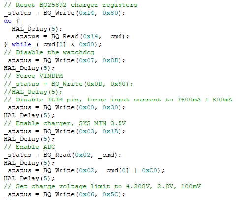
The initialization sequence that I'm using for BQ setup is:

After countless trials I came up with the above sequence, but the results are not quite good. The charging current is settled after a second o so at ~200mA. First, the charging current reaches ~500mA, but is drops immediately.

Another problem is that if the battery voltage drops to low ( < 3.8V) the charging process will not start. Sometimes the BQ gets stuck at system startup (both STAT and PG LEDs are poorly lit) and the TPS5420 enters in protection mode. Also, I guess when the charging process is about to be completed, the STAT led is blinking very fast and the voltage on the battery is jumping very fast between different values (4.01V - 4.15V).

I'm trying to figure out how the initialization sequence can be done right, any advices are more than welcome!

Bet regards,

Cristian

  • Hello Cristian,

    Can you please provide a register dump of the bq25892 (reg00-reg14) during the charging process?

    Looking at your code, I don't see anything inherently wrong, but I would like to see the rest of the status/fault registers.

    Cristian Dinca said:
    Sometimes the BQ gets stuck at system startup (both STAT and PG LEDs are poorly lit) and the TPS5420 enters in protection mode.

    Which protection mode is it entering? From the TPS5420 datasheet, I noticed there are 3 protection modes. I'm guessing it's going into over-current protection since it's a 2A buck converter (and the bq25892 input current is set to 2.5A) and GSM application typically have very dynamic profiles with high current spikes.

    If the TPS5420 is collapsing, the voltage at the input of the bq25892 will start dropping and recovering. One possibility of what's happening is that when the battery voltage drops into the fast charge region (3.8V is fast charge region), the input current demand will increase to support both the charging current + GSM load current. This is either throwing the TPS device into OCP due to the higher current demand or the bq25892 is going in input current limit/input voltage limit.

    We can verify this by monitoring the input voltage and seeing if VBUS is collapsing to UVLO and recovering, triggering the converter to try to start up again.

    Cristian Dinca said:
    The charging current is settled after a second o so at ~200mA. First, the charging current reaches ~500mA, but is drops immediately.

    Is this happening at start-up? If so, please monitor the SYS voltage. If the SYS voltage is less than 2.2V, the bq25892 will limit the input current limit to ~200mA to allow soft-start of the system rail.

    If not, the bq25892 could be in input current limit or input voltage limit at this point. The bq25892 will prioritize SYS current over charge current. So if the input is overloaded, it will decrease the charge current to allocate the input power to support the SYS.

    If possible, can you attempt to test the bq25892 bypassing the TPS device (e.g. apply 9V directly to VBUS using a DC power supply or adapter)?

  • Hi Fernando,

    Thank you for your reply!

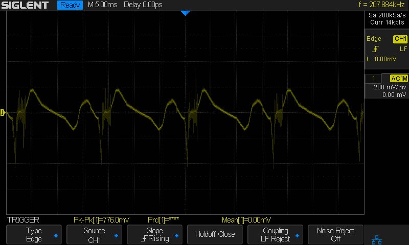
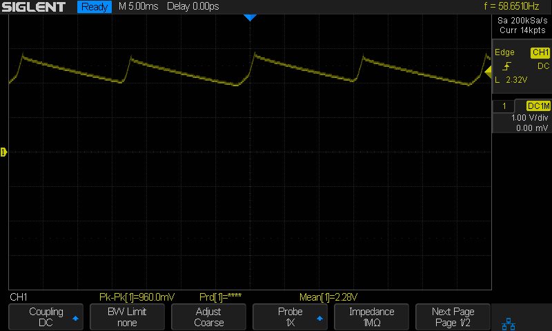
    I'm attaching the wave form of VBUS and SYS voltages during TPS collapsing:

    VBUS voltage average is around 9V.

    VSYS

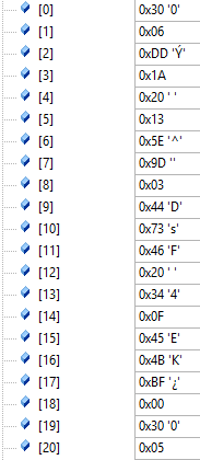
    Here are the BQ registers:

    What I didn't mention before is that the application is using a STM32F407 microcontroller which is powered from VSYS through a MCP1727-3302 voltage source.

    I have stopped the GSM module initialization and the problem remains. I think due to the low voltage of the battery (around 2.7V) which translates in a low VSYS voltage, the power needed to start the uC is not enough and the TPS is collapsing.

    I think I should set the charging current to a lower limit and do not allow the battery to go under 3.5V or so, but I don't know how to set this voltage limit.

    I don't understand why the system once is up and running, the charging current is not increasing, the uC is not getting more than 100mA and the power source is 2A.

    Regards,

    Cristian

  • Hello Cristian,

    Thanks for the information. I uploaded your register values to bqStudio and the main things I noticed are as follow:

    1. The part is in Thermal Shutdown reg0x0C = 0x20. This would explain why you are seeing no charge current.The device is most likely going in an out of thermal regulation/shutdown to prevent damage. If the bq25892 is in thermal regulation, it's possible the TPS device is also tripping its thermal protection. Are you using a TI EVM or a custom PCB layout? If custom PCB layout, please review the layout guidelines of the datasheet to ensure proper heat distribution on the PCB during operation (primarily the thermal pad of the device is properly grounded and the traces are correctly sized.)
    2. The watchdog timer isn't disabled, reg0x07 = 0x9D. Your code to disable WTD seems correct, so I would verify the STM MCU I2C engine isn't NACK'ing when trying to send this command. I noticed your other commands were successful.
    3. When there's an input applied and VBAT is less than your MINSYS threshold, the converter should regulate SYS to the MINSYS voltage (3.5V in your case). Since the device is in thermal shutdown, the converter isn't operational and can't regulate the output voltage. The waveform provided tells me that the voltage at SYS is just going from your battery voltage (RMS voltage is ~2.3V from the waveform) down to the BATFET's cutoff threshold to prevent over discharge. 

    Cristian Dinca said:
    I think I should set the charging current to a lower limit and do not allow the battery to go under 3.5V or so, but I don't know how to set this voltage limit.

    I recommend disabling charge first and verifying whether the device can start up, regulate the SYS voltage to 3.5V and power your system. The main issue is the thermal shutdown, this will prevent the device from operating at all.

  • Hi Fernando,

    My design is custom made, no EVM used.

    It is possible that I have made several mistakes when I have designed the PCB layout. The thin traces are less than 7mil.

    The system can startup just fine, the problem is the battery charging issue when the battery is too depleted.

    It is possible to set a minimum threshold on BQ for battery voltage, around 3.5V, to automatically shutdown the SYS? I want the system to shutdown when the voltage is too low, no need to continue the battery depletion. If not, I guess I can implement this using uC software and query the battery voltage from time to time and decide the shutdown.

    Regads,

    Cristian

  • Hello Cristian,

    Thanks for sharing your layout file.

    Yes, I believe your trace width is too small for high current forcing the charger into thermal shutdown. I recommend for your next revision to increase the width of the copper traces for power nets such as PMID, SYS, SW, BAT, VBUS and specially ground. If you can extend the ground pour that will be beneficial with the thermal dissipation of the IC; in particular the connection of the thermal pad. What we recommend for the thermal pad is to have the bottom layer or the 1st internal layer of the PCB (if using a multi-layer design) to be designated to GND only, this way you can put 6-9 vias on the thermal pad and connect them to the GND plane below directly. The reason the device is going into thermal shutdown is most likely because the thermal pad is only connected to GND via a single 7mil trace.

    Another critical net is the PMID net, as this is one of the high frequency current loops and the input to the actual DC/DC converter. Try to move the PMID decoupling cap as close as possible to the pin and have one short (but wide enough) trace to minimize the loop distance.

    You can use the EVM layout shown on the user's guide as reference. For QFN device, you can also increase your copper weight to 2oz for even better heat sinking capabilities of your PCB, but this is only if you don't share the PCB with WCSP devices, if so, 1 oz copper is enough.

    Regarding the under-voltage battery limit, there's not setting to change this. The functionality would need to be implemented with the host MCU + using the on-board ADC to read VBAT.