This thread has been locked.

If you have a related question, please click the "Ask a related question" button in the top right corner. The newly created question will be automatically linked to this question.

TPS65105: can't work normally

Part Number: TPS65105

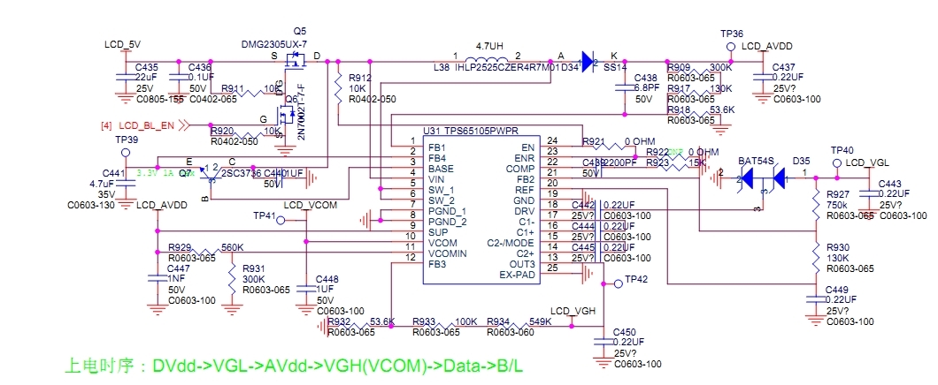
1. As the following schematic, set LCD_BL_EN as 3.3V, LCD_AVDD is about 4.8V. But VGH, VGL, VOM is almost 0,TPS65105 doesn't work.

2. When connect drain and source port of Q5 PMOS together,TPS65105 can work,AVDD, VGL, VOM is as the value expected.

 but VGH  is around 20V not as expected,remove C445,  and connect C2-/MODE  to ground, VGH is normal as expected.(16V)

So, what's the problems with this circuit?

  • Hi Chen,

    I have notified our expert regarding this topic. Please expect a response by 9/5/18.

    Regards,
    Aaron
  • Hi Aaron,

    Thank you for your concentration, I'm looking forward your reply.

    Best Regards,

    Chen

  • Hello Chen,
    I will only address your point 2 since it is related to TPS65105. When C445 is connected between C2+ and C2-/Mode pin, TPS65105 operates in voltage tippler mode and in this mode, irrespective of how the feedback divider network is set for VO3, the minimum voltage that VO3 (LCD_VGH in your schematics) can support is ~ 2 x VO1. Since your VO1 (LCD_AVDD in your schematics) is set to ~11V and 2x 11V = 22V. That is the reason you are getting the 20V for VO3 and not the 16V that you are setting with the resistor divider.
    When you remove C445, TPS65105 operates in voltage doubler mode and in this mode (with values set in your schematics) it is possible to obtain less than 16V for positive charge pump and that is why you are able to obtain the desired 16V output for VO3.
    Please review table 5 on page 22 of the datasheet to get further understanding of the minimum and maximum voltages that you can get from positive charge pump.
    Kind Regards,
    Liaqat
  • Hello Liaqat,

    I have checked the point you referred, and removed C445 and connected C2-/MODE pin to ground,

    but the testing data showed that TP65105 still not work, some voltages is as following:

    FB1: 0.54V
    FB4: 3.31V
    BASE: 3.34V
    VIN: 4.96V
    SW1: 4.96V
    SW2: 4.96V
    SUP: 4.96V
    VCOM: 0V
    VCOMIN: 1.65V
    FB3: 0V
    OUT3: 0V
    DRV: 0V
    REF: 1.21V
    FB2: 1.03V
    COMP: 2.79V
    ENR: 4.96V
    EN: 4.96V

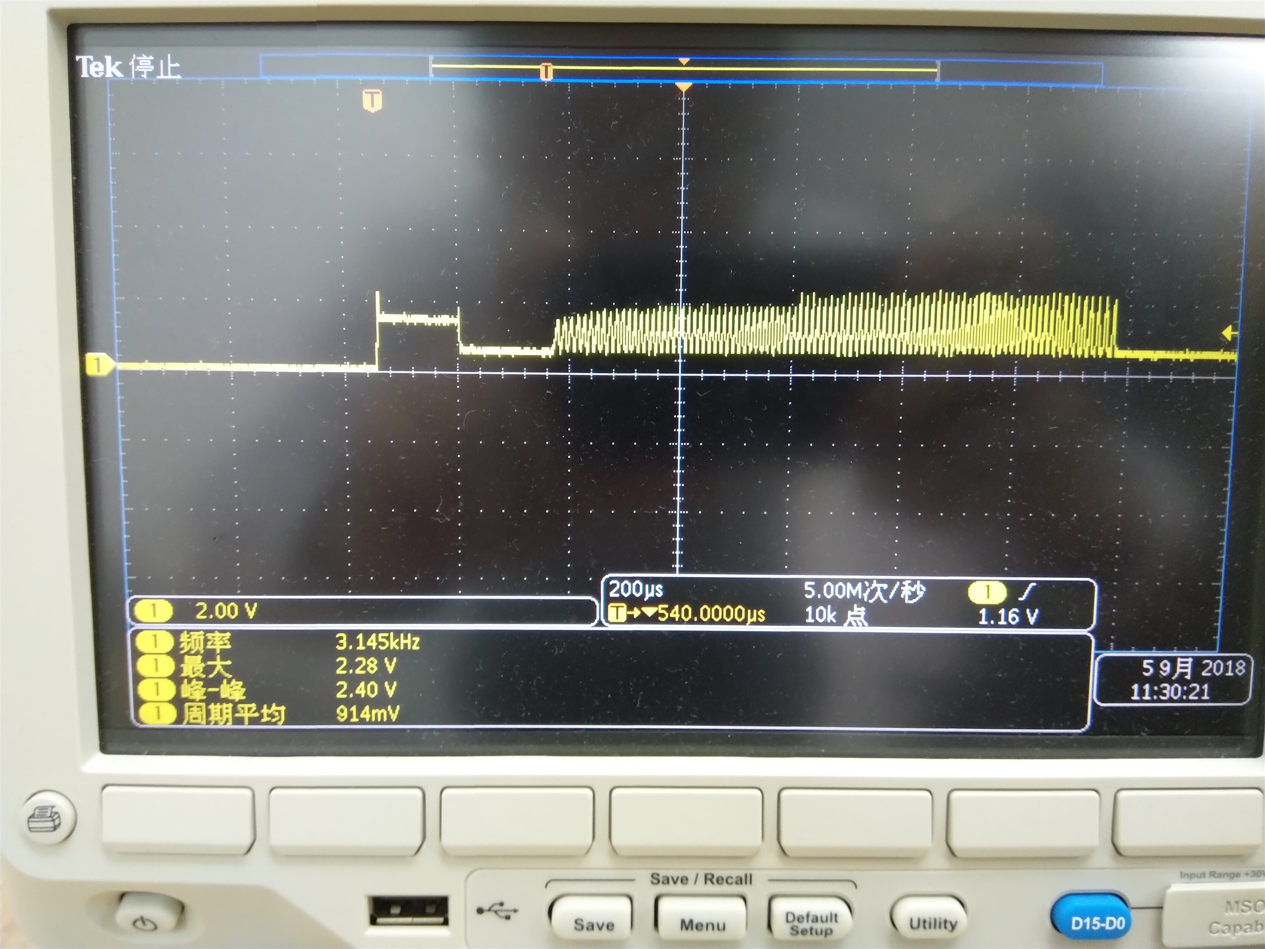
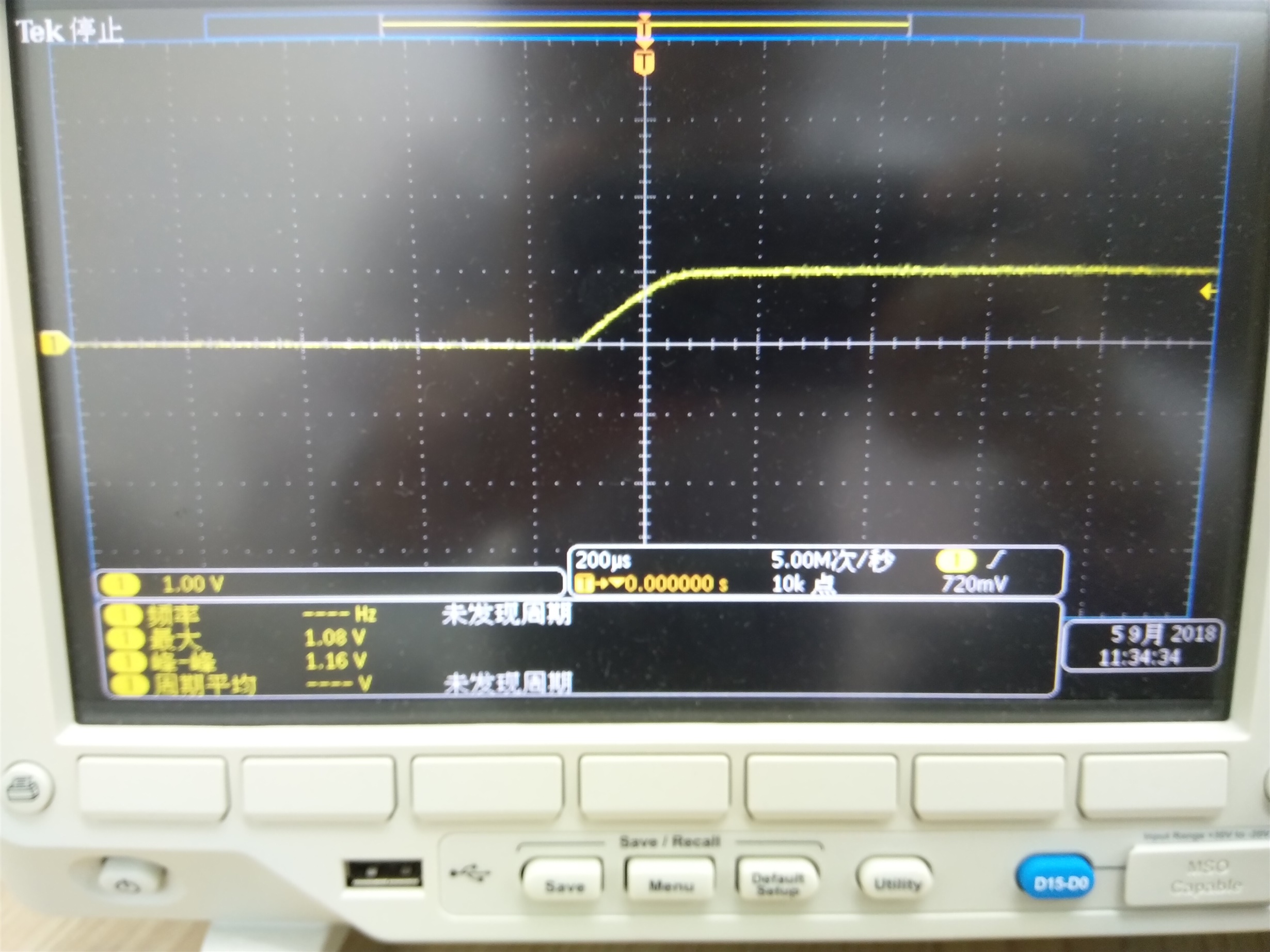
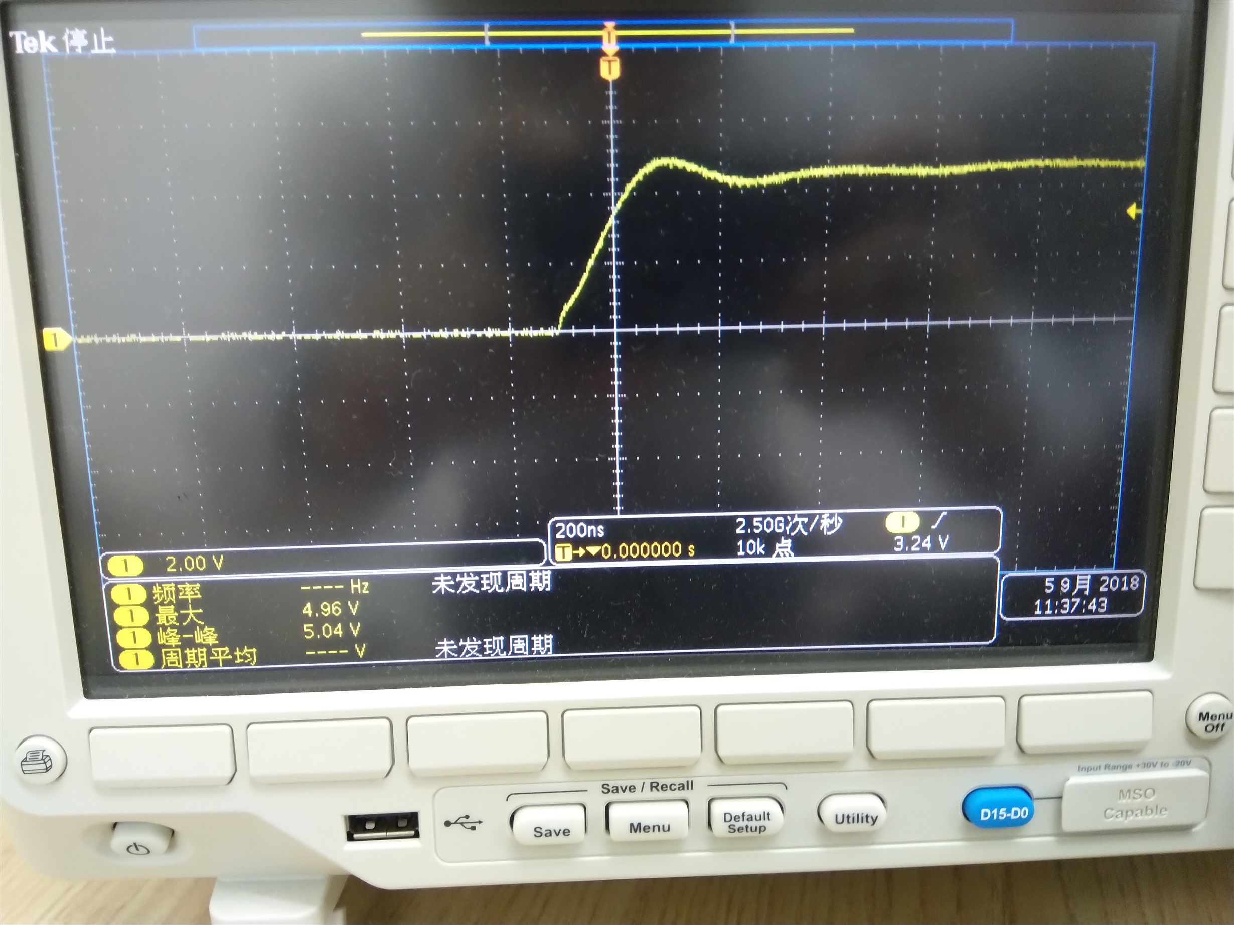
    And we have tested the start up waveform of LCD_AVDD, FB1, FB2, FB3 and EN, the waveform is as following:

    1. LCD_AVDD waveform, the voltage reaches the set value at first, then drop down and ringing at a frequency about 100KHz.

    2. FB1

    3. FB2

    4. FB3 is always 0V.

    5. EN

    So, could you help me to find out the reason why TPS65105 can't work?

  • Hello Chen,

    In the original post, the issue you mentioned related to TPS65105 was that VGH is 20V instead of expected value of 16V but everything else is working. So I explained to you the reason for why you are getting 20V for VGH rail. But from your latest post, it seems that the boost circuit is not working at all and you are not getting the proper voltages at other rails because of that. From your attached waveform, it seems that boost loop is unstable. I see that boost output capacitor is only 0.22uF and that could be  the reason for unstable loop. Recommended value for boost output capacitor is 22uF. Can you please change boost output capacitor C437 to 22uF and see if the instability goes away?

    You also seem to have sent a duplicate e-mail about the same issue so I will respond to that as well.. 

    Kind Regards,

    Liaqat

  • Hello Chen,
    Since we are discussing this via direct e-mail, I will close this thread.
    Kind Regards,
    Liaqtat