Part Number: BQ24650
Team,
our customer would need help with bq24650 layout:
"I have question about Battery Charger bg24650.
I design new PCB with bq24650 and I'm trying to do the best layout.
I read recommendations in technical documents SLUSA75A (datasheet) and SLUU444A (user's guide).
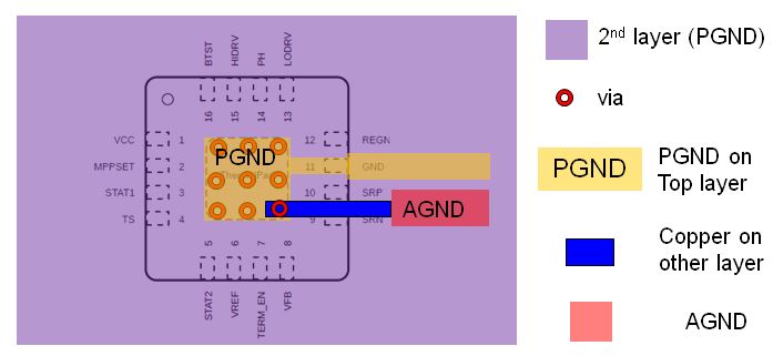
One of recommendation is "Route analog ground separately from power ground and use a single ground connection to tie charger power ground to charger analog ground.". That I understand. But I have problem with assignment pins GND(11) and ThermalPad to analog or power ground.
In datasheet SLUSA75A page 4 is write:
11 - GND - Power ground. Ground connection for high-current power converter node. On PCB layout, connect directly to source of low-side power MOSFET, to ground connection of input and output capacitors of the charger. Only connect to GND through the thermal pad underneath the IC.
Recommendation page 28 (SLUSA75A):
Route analog ground separately from power ground and use a single ground connection to tie charger power ground to charger analog ground. Just beneath the IC use analog ground copper pour but avoid power pins to reduce inductive and capacitive noise coupling. Connect analog ground to the GND pin. Use the thermal pad as a single ground connection point to connect analog ground and power ground together, or use a 0-Ω resistor to tie analog ground to power ground (thermal pad should tie to analog ground in this case). A starconnection under the thermal pad is highly recommended.
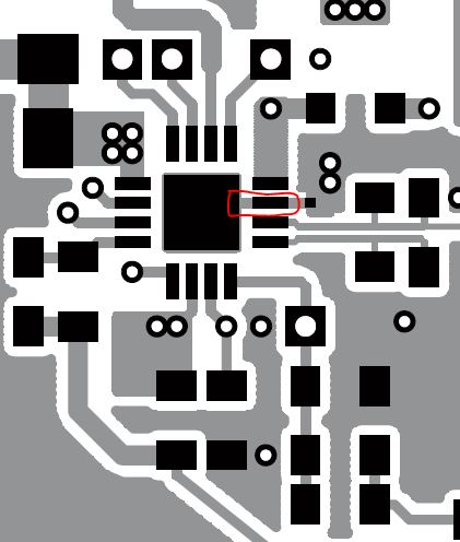
Page 22, figure 15 (SLUSA75A):
On the schematic is GND pin connect to power ground.
User's guide (SLUU444A) page 17, figure 8:
On the schematic is GND pin connect to power ground.
User's guide (SLUU444A) page 11 - 14, figure 2 - 5:
On board layout is GND pin connect to analog ground. Thermal Pad is connect to power ground.
- My question is, where should I connect GND pin and where Thermal Pad? What's the best? Is Board layout of EVM the most important recommendation?
Thank you for your help,
Kind regards,
Customer