This thread has been locked.

If you have a related question, please click the "Ask a related question" button in the top right corner. The newly created question will be automatically linked to this question.

LMG3410-HB-EVM: Idea for suppress heat LMG3410R070 Daughter card

Guru 19485 points
Part Number: LMG3410-HB-EVM

Customer is evaluating LMG3410-HB-EVM (and LMG3410-BB-EVM), but L2(inductor) was increased over 120℃ by thermograph.

User's guide is described that heatsink and airflow are recommended, but I think these idea is not critical for decrease L2 temperature.

(L2 was not decrease temperature)

Please let me know about two points question below;

①Is there proposed measures by L2 temperature?

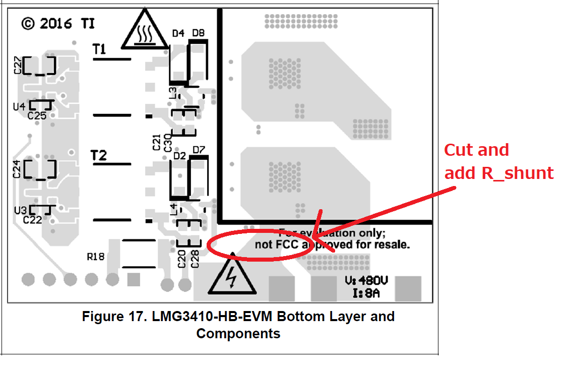
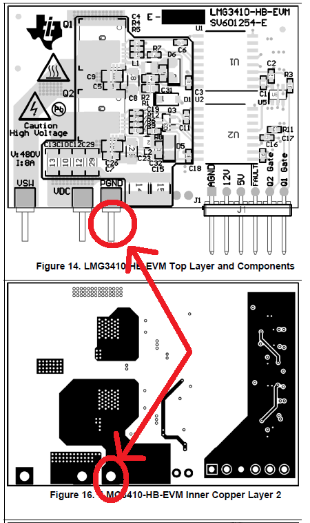
②Please let me know about measuring method for High-side GaN's drain current.

【Condition】

・Input(Primary): DC 400V

・Output(Secondary): 200V

・PWM: 5Vpp

ON Duty:0.3~0.5

・Pout: 35W(ON Duty:0.3)~100W(ON Duty:0.5)

・fsw: 50kHz

・Ta: about 20℃

Best regards,

Satoshi

  • Hi Satoshi,

    The hot inductor in your case may relate to the reasons below:
    1. The saturation current of this inductor 2300HT-151-H-RC is 7.5A, whose datasheet can be found below. With 5A average output current plus the ripple, the core may be saturated.
    www.bourns.com/.../2300ht_series.pdf
    2. Higher rms current will increase the winding loss, increasing the winding temperature.
    To solve the problem, we suggest you to change a different inductor here, or increase the switching frequency to lower down the ripple current. 100 kHz can be a good trial. The inductor temperature is close to 100C with 100 kHz.

    It is hard to use this EVM to measure the high side GaN drain current, because to achieve a low loop inductance, the GaN FETs and the DC bus ceramic capacitor locate closely on board. There is no space to put a shunt resistor in the power loop on the EVM.
    If you would like to design one board to evaluate the device drain current, here are my suggestions:
    1. A shunt resistor can be put in series with the low side GaN, though it will increase power loop inductance and affect the performance of the GaN FET a little bit.
    2. To measure high-side GaN drain current with the current shunt, be sure to use an isolated probe. A high bandwidth is also necessary to capture the high di/dt
    3. If you would like to use rogowsgi coil probe, please make sure the bandwidth is high enough.
    4. If you would like to check the switching waveforms under hard-switched condition, the low-side FET in the boost converter with the current shunt can provide the information. It is easier to measure current than to measure high-side GaN EFT Ids in the buck converter.

    Thank you!
  • Bingyao-san

    Thank you for reply,
    I will feedback to you if there any update.

    I have additional question,
    Is there test condition for below spec on LMG3410-HB-EVM and LMG3410-BB-EVM User's Guide?
    ⇒Input current, PWM input (Frequency and Duty), Load resistance, Output voltage and current
    www.tij.co.jp/.../snvu637.pdf

    Best regards,
    Satoshi
  • Hi Satoshi,

    You can refer the test condition shown in Fig. 11-13.

    Please let me know if you have more questions.

    Thanks,

    Bingyao

  • Bingyao-san

    Sorry for additional question, please let me know about two points below for snou140a User's Guide (Page 17 Layout);

    ①About your idea for measure Low side FET with current shunt, is below measure and connect R_shunt point correct?

     If incorrect, please let me know about correct point.

    ②Is below point isolated from PGND?

    Best regards,

    Satoshi

  • Hi Satoshi-san,

    For your first question to add the shunt resistor:

    1. The inner copper layer 2 also has the copper to connect the device source to the GND. If you want to cut the copper, you also need to cut the copper in the inner layer 2.

    2. The shunt is needed to added between the low-side FET and the bus capacitors, not just the GND terminal. The position pointed only cuts the connection from the FET source to the GND terminal, which will not give the low FET current information if the shunt is inserted.

    3. This method (cutting the copper and inserting a shunt) introduces large parasitic inductance into the power loop, which would induce large switching overshoot/undershoot. The results would not be true/optimal performance of GaN. It is suggested to build a new PCB with nice layout to include the current shunt

    For your second question:

    The termination you highlighted is connected to PGND. 

    Please let me know if you have more questions.

    Thank you,

    Bingyao