This thread has been locked.

If you have a related question, please click the "Ask a related question" button in the top right corner. The newly created question will be automatically linked to this question.

LMZM33603: Separating AGND and PGND?

Part Number: LMZM33603

Guys, I am working with a customer and have the following question on layout for the LMZM33603. 

The layout and pin descriptions say to keep AGND (zero reference) separate from PGND (power ground) on the LMZM33603.  Recommendation is NOT connect them together. BTW, this board also has an LMZ34002RKG on it.

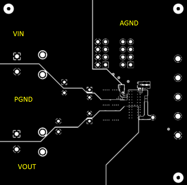
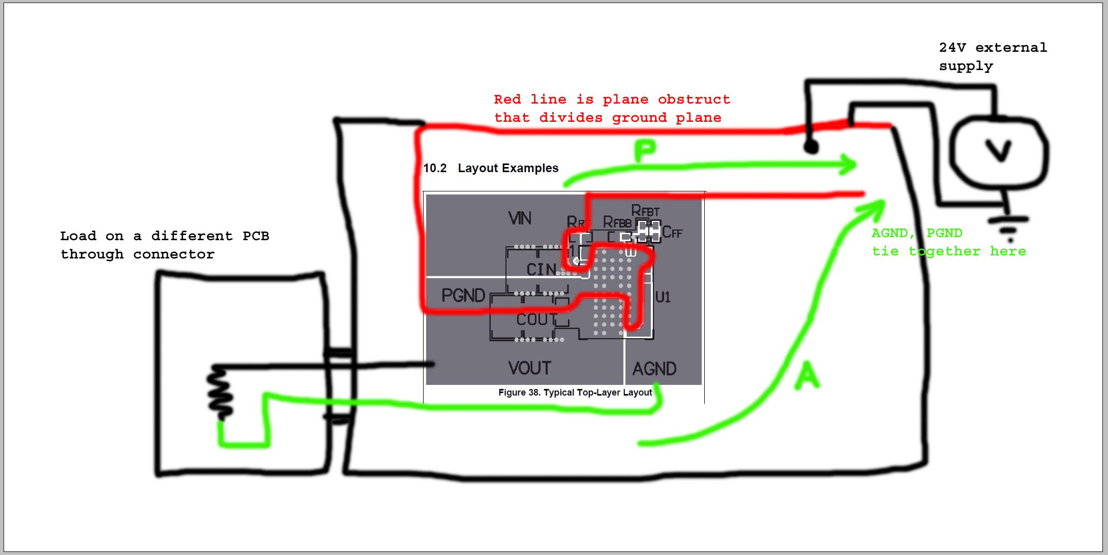
In the design, everything is referenced back to the input supply (24V wall wart) and chassis.  I think we can keep AGND isolated from PGND immediately in the vicinity of the LMZM33603, by putting a route obstruct between those planes.  this should help define return paths, but I don’t know if that’s adequate, because AGND and PGND do end up getting connected at the main supply a couple inches away. ATTACHED image has a rough idea of what the design will look like.

Questions:

1. Is this a big deal and how will it impact my performance?

2. Do you have guidance for using the LMZM33603 if it is not feasible to have isolated AGND and PGND planes?

  • Hi Kannan,

    The purpose of AGND is to have a dedicated GND plane away from the noisy PGND. The device has AGND and PGND are internally tied in this device. Ideally having these two planes separated similar to the EVM would be best. However I don't think there would be much risk with this layout since most of the fast switching current will go through the input capacitor instead of polluting the AGND. Can I ask why the layout as poured this way? If we can get the customers to isolate the two planes this would be most ideal. 

    An example of this would be the LMZM33603EVM Top Layer:

    Regards,

    Jimmy 

  • Thanks Jimmy. This makes sense. Will advise customer with the changes needed.