This thread has been locked.

If you have a related question, please click the "Ask a related question" button in the top right corner. The newly created question will be automatically linked to this question.

TPS56121: how to know the highside mosfet voltage withstand of the TPS56121?

Part Number: TPS56121

hi team,

how to know the highside mosfet voltage withstand? Whether it has risks based on the SW waveform? (The input is 12v) Need us to use the full bandwidth of the probe? Thanks.
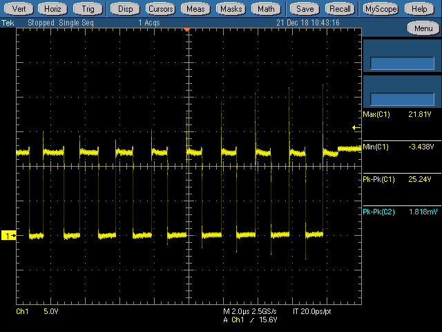
  • Frank,

    Generally you can look at the absolute maximum rating for the SW node in the datasheet, section 6.1 for TPS56121.  The actual breakdown voltage will be somewhat higher, but it is guaranteed up to the abs max limit, which is 25 V for TPS56121.

  • Hi John,

    i want to check the highside mosfet. Thanks. BTW: do you have some suggestions to test it?

    Thanks.
  • Frank,

    The SW absolute maximum voltage rating applies to both the high side and low side FETs When the low side is on, the full voltage is present across the high side. When the high side is on, the full voltage is across the low side. To test you could increase teh input voltage above the abs max until the device fails due to EOS. It will be permanently damaged at that point. As long as you maintain voltages below 25 V you are safe.
  • Hi John,

    Thanks. based on the datasheet, whether we need to use the input minus the negative SW to get the highside mosfet VDS?

    BTW: when we test it, do we need to use full bandwidth? how about 20M and 50M bandwidth?

    Thanks.
  • Frank,

    I would use the highest BW available or better yet a differential probe.  If using a regular probe make sure to keep the ground loop as short as possible (< 1cm).  The worst case stress for the high side FET is on the falling edge of the SW waveform when the high side turns off and the negative SW node transient occurs.  VIN minus the transient undershoot voltage is the voltage across the high side FET.  It should be less than 25 V.