This thread has been locked.

If you have a related question, please click the "Ask a related question" button in the top right corner. The newly created question will be automatically linked to this question.

UCC28251: full range adjustable output voltage

Part Number: UCC28251
Other Parts Discussed in Thread: UCC2897A

Dear All,

i approached to a hard switching topology for a wide range duty cycle application in several posts.

i selected the half bridge working with UCC28251.

the output voltage range is 0 to 40 V ( adjustable ).

the input voltage is 400 V ( form UCC28019A PFC stage ).

the maximum current is 10 A and the load is a  resistance ( variable resistance 400 W ).

please see the bellow schematics ( form data sheet ):

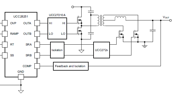
there is a ordinary transistor output optocoupler in the "feedback and isolation" block.

i have two questions:

1) can optocoupler work for the complete/wide range output voltage? in other words; is there linearity problem with such an output voltage range from 0 to 40V?

2) should i to worry about flux walking of the half bridge topology in voltage mode control?

Best Regards,

Ras

  • Hi Ras,

    Thank you for your question, I have asked one of my colleagues to help here.

    Regards,
    Teng
  • Hi Teng,
    thank you.
    also there is another question:
    is it possible such an adjustable full range ( 0-40V ) application with active clamp forward topology using UCC2897A ( up to 300W )?

    Best Regards,
    Ras
  • Hi Ras,
    For your questions, please see my reply as below.
    1) can optocoupler work for the complete/wide range output voltage? in other words; is there linearity problem with such an output voltage range from 0 to 40V?
    Frank: It is a valid concern. Although I believe the output voltage can still be regulated with non-linear opto-coupler, the wide range CTR of opto-coupler may cause loop gain variation across output voltage, which results in poor load transient performance and output accuracy. So, it is better to put UCC28251 on the secondary side to remove opto-coupler. For the design of minimum output voltage such as 0V, you need to put consideration on UCC28251’s minimum on time which is known as blanking time in the datasheet.
    2) should i to worry about flux walking of the half bridge topology in voltage mode control?
    Frank: You need not to worry about it.
    3) Is it possible such an adjustable full range ( 0-40V ) application with active clamp forward topology using UCC2897A ( up to 300W )?
    Frank: It is difficult because the resonant cap’s voltage in ACF topology and transformer’s winding voltage that is used for SR gate drive are both relevant with output voltage. So, wide range of output voltage makes it complex and difficult to design.

    Regards
    Frank
  • Hi frank,
    thank you for the reply. my questions are answered.

    i have three other questions:
    1) can i think about two switch forward topology for my application ( full range adjustable )?
    2) i am confused about duty cycle limitation of the full bridge topology. does the maximum of it equal to 50% or 100%?
    3) how does UCC28251 prevent/compensate the flux walking/capacitors voltage unbalance?

    Best Regards,
    Ras
  • Hi Ras,

    For your additional questions, below are my thoughts.

    1) can i think about two switch forward topology for my application ( full range adjustable )?

    Frank: yes, but its efficiency is lower than HB.
    2) i am confused about duty cycle limitation of the full bridge topology. does the maximum of it equal to 50% or 100%?

    Frank: The effecitive duty cycle is close to 100% if you simplified the Full-bridge topology to a buck.

    3) how does UCC28251 prevent/compensate the flux walking/capacitors voltage unbalance?

    Frank: In normal operation, there is no voltage walking aournd on bridge caps' voltage. It normally occurs under cycle by cycle current limit condition. UCC28251 avoid it from happening by forcing the duty cycle of low side and high side MOS be equal.

    Regards

    Frank 

  • Hi Frank,
    thank you. my questions addressed excellently.
    please, if possible, tell me about:
    1) the effective duty cycle ( full bridge ); how does it occur?
    2) how to simplify full bridge to buck?

    Best Regards,
    Ras
  • Hi Ras,
    If you put buck topology and full-bridge into comparsion, you may find both topologies leverage output inductance(L) and ouptut capcitor(C) to convert the square wave input voltage to DC output voltage. The so-called effictive duty cycle in my previous post refers to the duty cycle of square wave which is the input voltage of the output LC filter. For buck, it simply equal to the duty cycle of high side MOSFET. And for hardswitcing full-bridge topology, it is rougly equal to two times of the duty cycles of primary switches.

    Regards

    Frank