This thread has been locked.

If you have a related question, please click the "Ask a related question" button in the top right corner. The newly created question will be automatically linked to this question.

TPS23754: Some circuits are different with TPS23754EVM-383

Part Number: TPS23754

Dear Sir,

This is Gordon Liu of WNC.

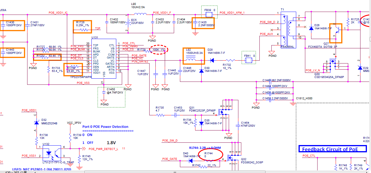
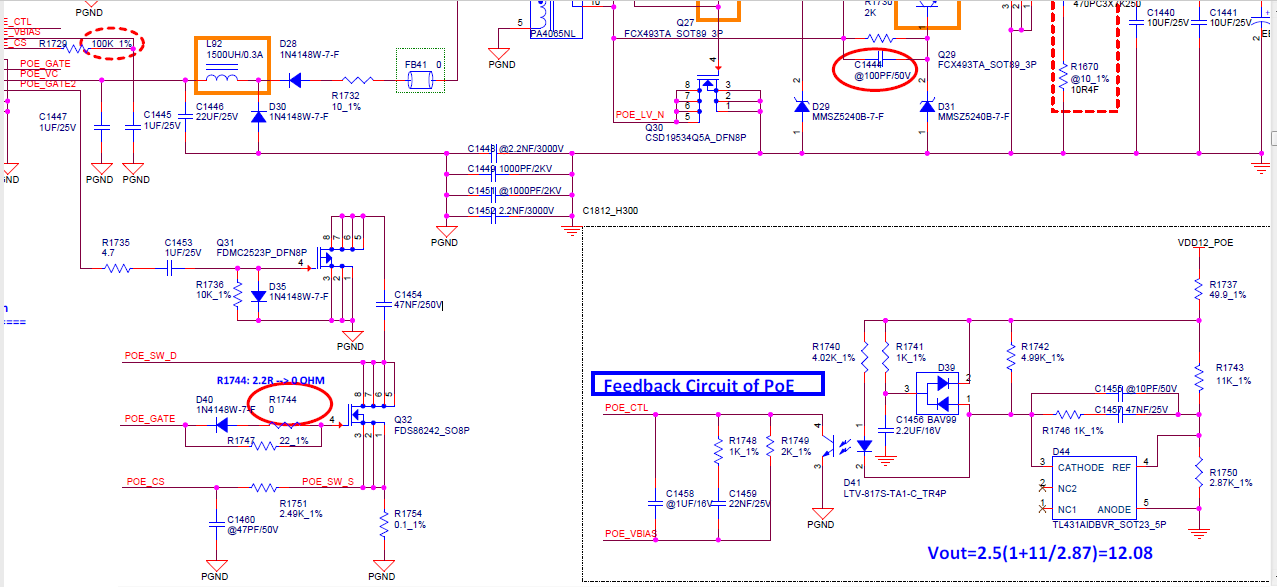
I get a a POE schematic which is almost copy the  TPS23754EVM-383 circuit.

I find out 2 different circuits but I can't understand what it is used.

Could you give me any concept base on you professional ability??

1: R1729=100K, C1445=1uF;  Why the CS pin need to pull-high from the VB??

2: C1458=1uF; it create a big pole point on the feed back circuit. does it make sense??

BRs,

Gordon Liu

  • Hi Gordon,

    Could you post the PDF of the schematic? You can share it here or via direct message.

    Thanks,
    Tom Amlee
    PoE PD Apps Engineer
  • Hi Gordon,

    1. The resistor from Vb to Cs is there to pull up the Vcs voltage so that it will reach the Vcs max threshold (0.55V) sooner, limiting the primary side current. As configured the peak primary current would be 4.3A. If the Vb pull up was not there, the peak primary current would be 5.5A.

    The design of the circuit likely added R1729 because they had a limited selection of current sense resistors. Typically, one would just increase the value of the current sense resistor to limit the primary current.

    2. We sometimes add an additional pole here to additionally attenuate high frequency, so I  would expect something in the nano-farad range, not 1uF. The designer may have placed the 1uF here mistakenly since the TPS23754EVM-383 schematic has the Vb bypass cap (C16) in a similar location, but connected between VB & RTN.

    For more guidance on feedback component selection, take a look at section 2.8 & beyond of slva305c.

    Regards,
    Tom Amlee
    PoE PD Apps Engineer