This thread has been locked.

If you have a related question, please click the "Ask a related question" button in the top right corner. The newly created question will be automatically linked to this question.

TINA/Spice/LM5085: Gate Drive MAX current. Spec. versus model

Part Number: LM5085
Other Parts Discussed in Thread: TINA-TI, , LM5145, INA169, LM5117

Tool/software: TINA-TI or Spice Models

Hi,

Whilst busy inside simulations using LM5085 I noticed that I was seeing significantly higher switching losses from the power FET and investigated. I have generated a few questions.

Q1. The Datasheet for the LM5085 states that the gate drive is capable of ~1.5A and has an output Resistace of 2.3ohm (@500mA). However I noticed that the Spice model shows gate currents of only 150mA. I tested this both whilst driving the FET and to be sure I strapped the gate output to Vin through a very small resistor to see what current the gate pin would sink when the converter attempted to start. ~154mA. This is much much lower than expected. Can anyone explain?

In an attempt to see how that converter would perform with more reasonable gate currents, I followed the gate output with a BJT push pull pair between Vin and Vcc, using some high speed BJTs, the affect was dramatic. The gate drive current on the active side of the PP pair jumped as expected to >1.5A peak. Switching times significantly improved and the efficiency jumped up 'a lot'.

The lower leg of the PP pair was connected to Vcc, therefore this 1.5A was being sunk into the Vcc pin.

Q2. Would the real IC actually allow such currents to be sunk into the Vcc pin? The datasheet states Vcc Current limit at 40mA, but it does not state sink or source. I strongly assume this configuration would be invalid.

In the process of doing this I noted that the datasheet states, "The regulator is disabled when the LM5085 is shutdown using the RT pin". When I shutdown the model in this way the Vcc pin stays nailed at Vin-8V.

Q3. I assume that with the real IC, when in shutdown, Vcc would float up to Vin rapidly. Can you confirm this?

Finally can you comment on the idea of following the gate output with a higher power driver. like I described. I'm hoping that this is just not necessary, but the drive I'm getting from the Spice model is just not enough.

I am designing a 60V in....42-60V current regulated converter, capable of 8A output at any voltage between 42-60V. That's around 400W as a system. Looking at the datasheet it is almost impossible to predict efficiency, but using simulations I am surprised at the results. I have designed the converter to run at around 60Khz, in an attempt to reduce switching losses, which as expected predominate. Even so, with the LM5085 as the sole gate driver I am seeing between 10-20W power dissipation in the PFET, depending on the particular FET I use. When I drive the gate with an auxiliary driver I can reduce this power loss to < 3W. This makes a huge difference to the package type and heat-sink requirements of the PFET.

This is an awful lot of simulation and not much reality, but I would appreciate any feedback on my questions and comments on the application.

Many thanks

Aidan

  • Hello Aidan,

    I have forwarded your questions to the product expert, and he will follow up with you.

    Best Regards,
    Katelyn
  • Hi Michael,

    Q1. Gate driver current rating is typically a peak current measured with a capactive load.

    Q2. Gate drive current is only at the switching instances - the DC level is much lower than the peak required to charge nd discharge the gate.

    Q3. Yes, VCC cap voltage would decay.

    Q4. An external gate driver should not be required. However, based on the load current spec of 8A, I recommend using a synchronous controller suuck as the LM5145. The freewheeling diode losses in a non-sync solution will be too high.

    Regards,
    Tim
  • Thanks.....

    Q1&2, understood peak, but the model delivers the same 150mA peak (at the point of switching) and also 150mA DC. So I think this cant be correct.

    Q3. Decays towards Vcc I assume. NOT towards GND. Also the model does neither. So please be 100% clear as I am considering using Vcc as a ref for an external follower to drive the bottom end of this PP pair. I need to know what it does when the device is switched off via RT.

    Q4, Its not too suitable to use a sync controller. The problem is that this is a battery charger, My supply Vin will never be higher than the absolute max charge voltage of the battery and I must charge to the same voltage as Vin. If I use a sync controller, I will always loose a few volts between Input to Output (quite a significant voltage in fact). I trawled your many sync controller and with Vin @ 60V none can deliver more than 57V output. I do not want the complexity of a boost controller or LLC, if I manage the power well with the LM5085, it can be quite simple.. That has been my thinking anyway.

    However the most important point of my question is this apparent current limit that I see on the GATE pin of the LM5085 model. I never see any peak current that comes close to the spec sheet and its making a huge difference to efficiency.
    Aidan
  • Thanks, Aidan.

    Q1 & Q2: I will ask our modeling team to verify the model's behavior.

    Q3. VCC is a floating rail referenced to VIN (VIN - VCC is regulated to 7.7V), so the VCC rail will converge to VIN after shutdown (going to GND would cause an overvoltage condition on VCC). The block diagram in the datasheet indicates that the VCC regulator is disabled if RT is pulled low.

    Aside: Figure 24 of the datasheet shows a Schottky diode from VCC to GND to prevent VCC going negative during low input voltage conditions (less than 8V input -- probably does not apply in your case).

    Q4. Yes, the LM5085 is suitable for high duty cycle conversion (VOUT close to VIN). There is an external circuit required if you need constant output current capability. The other option is the LM5145 -- its Toff-min spec is 140ns typ, 200ns max -- this sets the max duty cycle when operating in dropout.

    Regards,

    Tim

  • Thanks Tim,

    Yeah, actually my question about the Vcc output going to Vin was pretty dumb actually. After all if it did not pull towards Vin you will kill PFETs as soon as Vin was above 20V or so. Duuuh.

    Actually I looked at the LM5145 but still I came back to the LM5085. The lack of compensation issues and simplicity makes it attractive as I need to modify the design already to be CC only and not CCCV. I have studied your application note, (AN-2157), about using the current control feature within the LM5085, but actually this proves to have less than ideal operating characteristics in my scenario. The over current control in the LM5085 causes the IC to enter a backoff mode (forced off-time). This drives the frequency of the converter down and makes it difficult to control the operating frequency and efficiency if this is used as a primary regulation method.
    Instead I am trying, and it seems to work quite well (again in sim), the addition of an INA169 high side current monitor, then using the output from this to drive the FB pin of the LM5085. In this way the output current is controlled much more smoothly and operating frequency is predictable and changes proportionally with the difference between Vin and Vout.

    Still you are correct about the flyback current. I'm dumping over 2.3W in the current design. I got this down (sim of course) to 1.75W by using FERD rectifiers. Never tried them in this position, but I don't currently know of any reason why they are not a good option. Yet still HOT!
    Truth is the same is true for the PFET also. I am trying to get below 5W at full load in the PFET. But with the LM5085 (model) driving the FET, it's over 22W in the PFET Ouch!

    Yes its a lot of heat and maybe finally the sync approach might be better, however I say again drop out voltage is critical in my design. This drags me kicking and screaming back to the LM5085.

    If I use a simple PP augmentation and drive with BJTs at around 1.5A peak, the PFET power drops to 3-4W. Workable.

    However.........

    I again can confirm that I can not get more than 150mA output current from the IC in simulation. The datasheet says 1.5A peak. Where is it?

    Aidan
  • Aidan,

    Also consider the LM5117 as it has the current monitor output pin that is useful for constant current applications. However, its toff-min spec may not be low enough.

    The gate driver current spec is in the EC table of the LM5085 datasheet (1.75A source, 1.5A sink). 22W in the PMOS FET is way too high - please check the selected device in terms of conduction and switching losses  - the total power dissipation should generally be less than 1W in a 5 x 6mm package.

    Also, the LM5085 as a COT converter needs a certain amount of triangular ripple injected at the FB pin - this can be provided using a type 1 network (resistor in series with the output cap). Given the large difference from Vref to Vout however, a feedforward cap may be useful to couple the full output voltage ripple amplitude to the FB pin (i.e. type 2 network).
     
    Regards,
    Tim

  • Hi Aidan,

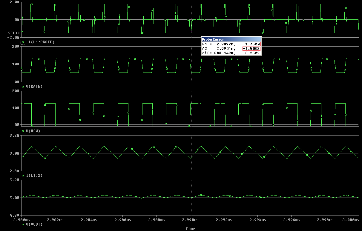
    Thanks for the feedback. We have implemented the Gate Driver Output Source/Sink currents properly. Below is the steady state simulation result of released test bench. To test peak source/sink Gate currents, we have connected additional 20nF capacitor at Gate node to Ground.

    Simulation Result: 


    [NOTE: I(U1:PGATE) and V(GATE) are the current through and voltage at PGATE pin respectively].

    Also, could you please attach your test schematic here? This will help us to analyse the issue regarding VCC pin current.

    Thanks & Regards,

    Arpan Gupta 

  • Hi Arpan,

    Thanks for getting back to me. Hmmmm, this is not what I am seeing. Whats going on I wonder. I have also tried adding 20nF and more to the gate just to try and drag something out of the gate pin. Nothing works. 150mA and that's it.

    I have attached my schematic. Please excuse the slow sim times, but much else is going on here. Still you will see around the LM5085 pin that I have implemented a BJT PP pair to get the currents I need. 

    For your purposes I have quickly taken the BJTs out of the equation and also added 20nF of extra gate capacitance on the 5085 gate pin.

    Take a look at G_5085_I and you will witness the lack of drive current. If you instead drive the BJTs with the 5085 you will see reasonable gate currents.

    All the best

    Aidan

    LM5085_Charge_Current_Limiter.tsc

  • LM5085_Charge_Current_Limiter_with_TINA_model.tscExtra,

    As a side note, but one that is still unanswered. The file I attached originally uses a slightly modified version of your unencrypted PSpice model. The reason for the modification is that the current limiting does not work when using higher input voltages to the IC. You will find my comments on this and comments from others who also seem to see the same problem. I made a small SPICE mod. to workaround this.

    However in my final design this was not critical, as I ended up using n external current monitor, therfore my macro mods where not so important.

    However to make sure that the behaviour I am seeing regarding gate current is not related. I have attached another schematic with the encrypted TINA Transient model included.

    As you will see. Same issue. 150mA drive current and no more.

    again all the best

    Aidan

  • Hi Aidan,

    Gate driver output Source/Sink currents are not modelled in the model you are currently using. Therefore, you will not be able to see proper results. Now we have implemented Gate driver output Source/Sink currents in the model. We have shared the updated simulation result with you on 07FEB2019. The updated behaviour will reflect after we release the updated model to TI website.

    Currently we are resolving the current limit issue for higher input voltage cases. You will find updates on this at below thread.

    https://e2e.ti.com/support/power-management/f/196/p/755044/2854404#2854404

    We are trying to resolve the current limit issue as soon as possible and targeting to release the final updated model (with both bugs fixed) by end of this month.

    Thanks & Regards,
    Arpan Gupta

  • Thanks Arpan,

    Good news. I have been now days working on the gate drive issues, with the assumption the IC will not deliver enough drive even if the model is realistic. However I think from the thermal perspective of the switching FET, so long as it can deliver around 800-900mA and do that through the Miller plateau, I will keep power loss under control. If I'm not mistaken the IC is likely to be better than using BJTs but your block diagram of the LM5085 does not show if the output stage is MOSFET based or not. Even using high gain NPN in my buffer, I still fall short when driving through the flat and this is where I'm generating most of the heat....of course.

    So, I'm glad your model is coming to success. Perhaps you can tell me if the IC actually uses MOSFETs in its output stage? Also is there any possibility, perhaps by sharing with me directly via email, that I can test your current updated model in my simulation. I realise it has not yet been released, but still...if I can be more confident of its behaviour, I can move on and begin laying out the PCB. Otherwise, you have me waiting until I have a reasonable idea if I truly need a gate drive buffer or not. So long as the model works at higher Vin, I'm not so concerned if its current limiting is not accurate, as in fact, I only implement overcurrent protection as a safety feature, as you will see from my schematic, the primary loop control is current based using an external high side current monitor. So when the circuit is operating normally the LM5085's current control is not actually triggered.

    Also, I will need to carefully consider the extra power dissipation in the LM5085 if it drives the gate directly. Although I'm not too worried at the moment a quick calculation suggests around 650mW from the IC. Not to be ignored and clearly I need to understand this before I lay out the PCB. So anything to help me move along would be a great assistance.

    All the best

    Aidan

  • Hi Aidan,

    We cannot share the updated model through email. You will get the updated model when we will release it to TI website. Sorry for the inconvenience.

    Thanks & Regards,
    Arpan Gupta
  • Thanks Arpan,
    So, you indicated at the end of the month. Can you tell me if this is actually still true. It would be great to test with an updated model.
    Thanks
    Aidan
  • Hi Aidan,

    Initially we thought of releasing the updated model by end of the month. Considering our current bandwidth, we might not be able to release the model by this month. But we will try to release the model as soon as possible. For now we are not committing any date but we will inform you once the model is released to web.

    For now we are closing the thread. Sorry for any inconvenience.

    Thanks & Regards,
    Arpan Gupta