Because of the Thanksgiving holiday in the U.S., TI E2E™ design support forum responses may be delayed from November 25 through December 2. Thank you for your patience.

This thread has been locked.

If you have a related question, please click the "Ask a related question" button in the top right corner. The newly created question will be automatically linked to this question.

UC1708-SP: UC1708 INPUT pin characteristic and isolated PWM signal stability

Part Number: UC1708-SP
Other Parts Discussed in Thread: UC1708

Hello

In my circuit, I use UC1708-SP driver. I added my schematic.

INPUT pin characteristic of UC1708-SP is really interesting. UC1708-SP IN pin behaves like a voltage divider from its isolated supply and some capacitance inside.

I also couldn't understand ENABLE pin characteristic.However, it works properly as schematic.

The block diagram in datasheet is insufficient to understand the input characteristic.

Attached schematic works however, circuit is sensitive and the power consumption from isolated supply is higher than 5W. However, there is just 20C temp. rise on UC1708-SP which is normal I think.

Could you please;

*please review design

*please explain INPUT pin characteristic

*please explain why there is a need 910R from INPUT to ISO.SGND. When I use higher than 910R at INPUT pin, in condition of PWM goes continously low, INPUT pin detects PWM signal as high and turns on MOSFET. (Circuit works reversely.)

*please explain why the series resistance 8.2R is good for INPUT pin, higher than 47R the driver signal is very bad and converter doesn't work properly.

*please explain what is the reason of high power consumption maybe the system is damped on 910R or 8.2R.

*Please, offer interface for INPUT pin for isolated PWM supply.

Thank you.

  • Hey gG,

    1. I would not keep the shutdown pin floating, but otherwise the schematic looks fine.

    2.When the Input goes high the BJTs turn on and when it is low the BJTs turn off. Is there anything else needed?

    3/4. The resistors are used to damp spikes on the line to protect the input of the device.

    5. Is it high power consumption? I don't believe the input resistors would cause the IC to draw more power. Often the power draw comes from whatever FET the driver is driving.

    6. Is there something wrong with your current input?

    Thanks,

    Daniel

  • Hello Daniel,

    1. OK. we will connect shutdown pin directly to GND.

    2. Yes, basically. However, we faced with a problem with INPUT pin. When we put 10kohm resistor instead of 910ohm, system doesn't work properly. Although duty signal coming from PWM driver is LOW state, the INPUT pin stays at 1.6V which is greater than the turn on threshold voltage of driver IC. Therefore, high side mosfet turns on continuously, despite the fact that it is supposed to be OFF when the duty = 0.

    3. Actually, 910R isn't in line. It is connected between INPUT pin and ISO.SGND. I think 910R doesn't play role to damp the signal . However, it reduced DRVR signal voltage on INPUT pin. Also, see 2.

    4. The 8R2 is in line. When we increased 8R2 to 47R, the gate signals malfunctioned and misoperation occured. We even couldn't monitor the signals. We need to turn off the system and 1708 heated up immediately.

    5. Power Supply of 1708 is 4W rated and 5W as maximum. At higher power, the converter reduces its output voltage.

    When our SMPS supply voltage isn't provided, the supply voltage of 1708 is 15V and gate signals are good at MOSFET.

    When we supply input voltage and SMPS works at rated power, the supply voltage of 1708 drops down from 15V to 10V. (MOSFET gate signal amplitude becomes 10V.)

    However, we don't think that gate drive loss of MOSFET is that much big.

    We are waiting for your explanations. Thanks in advance.

  • Hey Gg,

    2/3. I skipped over the fact you were using a transformer for the isolated signal. The transformer can be seen as an ideal current source. Increasing the 910 resistance to 10k will cause the "low" signal threshold to increase. Its likely you have to stick with the 910.

    4. Since the transformer is an "ideal" current source you need a current liming resistor there to help make sure our device doesn't take in too much current. 8.2 is a weird value, but generally I have seen this value in the 10s of ohms so its not crazy.

    5. That is way too high I agree. Lets see if there is a way to fix that.

    Also while we are at it I would suggest disconnecting the 200 kOhm resistors on the NC pins.

    Can you provide me with what FET you are using so I can figure out the drive needed to run the FET? (Datasheet will also work)

    Thanks,

    Daniel

  • Hello, 

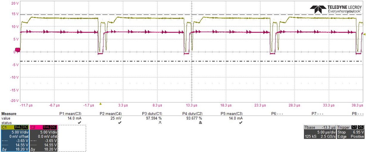
    Based on my schematic, I added the oscilloscope waveforms.

    MOSFET is JAXA 2SK4051.

    Condition #1: Power isn’t supplied to power stage. But all other control system is energised.

    In below figure is related to Condition #1, RED: UC1708-SP INPUT A signal, YELLOW: MOSFET Vg-s signal

    Condition #2: Power is supplied to power stage and all system is energised.

    In below figure is related to Condition #2, RED: UC1708-SP INPUT A signal, YELLOW: MOSFET Vg-s signal

    .

    Please review the waveform.

    a. Could you please comment on why INPUT A signal plateau voltage is near 10V despite PWM signal is between 0V and 15V?
    b. Could you please comment on the INPUT A signal drop when converter delivers power to load?
    c. Could you please comment on why DC-DC supply is down to 9V when converter delivers power to load?
    d. Could you please evaluate the drop at INPUT A pin by checking above schematic?

  • Hey Gg,

    a. the PWM signal is not dependent on the voltage of the input signal. Its dependent on Vcc.

    b. It looks like whatever is driving that signal may need more drive for the initial turn on of the internals of the UC1708-SP

    c. The IC pulls power from Vcc to turn on and off the MOSFET so as it pulls power, depending on what Vcc is connected to I would expect a drop.

    d. This is the same as question B

    Thanks,

    Daniel

  • Hello,

    a. The PWM signal is between 0V and 15V, and I transfer this signal from isolation transformer via shown circuit. Therefore, the red coloured INPUT A signal is dependent on the PWM signal amplitude. I would monitor INPUT A signal between 0V and 15V however, it is 0V and 10V. Could you please review again?

    b. Is there any application note about the layout offer for 1708?

    c. Is there any application note/schematic about the INPUT A configuration with isolation transformer config?

    After above waveforms, I made another test named as Condition #3,

    I just moved 8R2 resistor in series with the 1uF which is at transformer secondary and I observed below waveform.

    Condition #3: 8R2 is just moved to left between capacitor and diode as explained above, Power isn’t supplied to power stage. But all other control system is energised.

    RED: UC1708-SP INPUT A signal, YELLOW: MOSFET Vg-s signal

    d. Please, evaluate the above waveform for condition #3.

    Best regards

  • Hey Gg,

    Sorry I thought we were talking about the UC1708 device
    I would expect that the output of a 1:1 transformer with 15 V signal on the input by 15 V.

    The fact you dont see 15 V means there seems to be something wrong with your transformer.
    I dont have much to offer you about how to implement this circuitry better.

    Are there any issues you specifically have with the UC1708?

    Thanks,
    Daniel
  • Hello,

    Thank you.

    a. Is there any application note about the layout offer for 1708?

    b. Is there any application note/schematic about the INPUT A configuration with isolation transformer config?

  • Hey Gg,

    There is no application note talking about layout or schematic with the isolation transformer config.

    Thanks,

    Daniel

  • Hello,

    Thank you Daniel.

    a. Is Pwr Gnd A connected to  Pwr Gnd B inside of UC1708A-SP?

    b. Is Pwr Gnd A connected to  Logic Gnd  inside of UC1708A-SP?

    c. Is Pwr Gnd B connected to  Logic Gnd  inside of UC1708A-SP?

    d. How much is the Input A and Input B impedance? Are they all high impedance?

  • Hey Gg,

    a b & c) All the grounds while not necessarily connected will have ESD protection in between them meaning the grounds cannot have large votlage differentials between them.

    d) Note while "high impedance" the leakage current is quite high

    Thanks,

    Daniel